


TPU (Tensor Processing Unit) Deep Dive
I've been working with TPUs a lot recently and it's fun to see how they had such different design philosophies compared to GPUs.
The main strongpoint for TPUs is in their scalability. This is achieved through a co-design of both the hardware side (e.g. energy efficiency and modularity) and the software side (e.g. XLA compiler).
Background
To give a brief tldr on TPUs, it's Google's ASIC that focuses on two factors: extreme matmul throughput + energy efficiency.
Their origins go back to Google in 2006, when they were first evaluating whether they should implement either GPUs, FPGAs, or custom ASICs. Back then there were only a few applications that necessitated specialized hardware and they decided those needs could be met by bringing in excess CPU compute from their large datacenters. But this changed in 2013 when Google's voice search feature ran on neural networks and internal projections speculated that they would need much more compute if it took off.
Fast forward to today and TPUs power the majority of Google's AI services. Of course, that includes training and inference of Gemini or Veo, but also deploying their recommendation models (DLRMs).
Let's dive in and look at TPU internals from the bottom up.
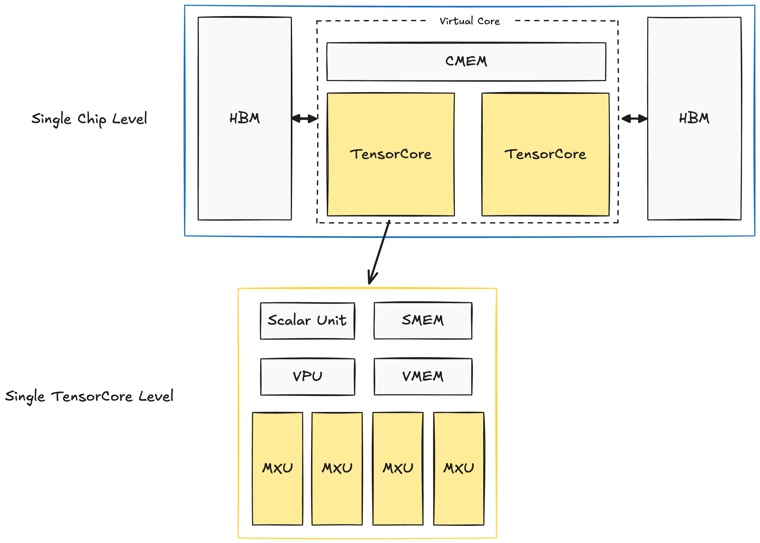
TPU Single-Chip Level
I'll focus my diagrams to TPUv4, but this layout is more or less applicable to latest generation TPUs (e.g. TPUv6p "Trillium"; TPUv7 "Ironwood's details aren't released as of writing in June, 2025).
Here's the layout of a single TPUv4 chip:
In each chip, there's two TPU TensorCores, which are responsible for our compute. (Note: inference-specialized TPUs have only one TensorCore). Both TensorCores have shared memory units: CMEM(128MiB) and HBM(32GiB).
And within each TensorCore, there lies our compute units and smaller memory buffers:
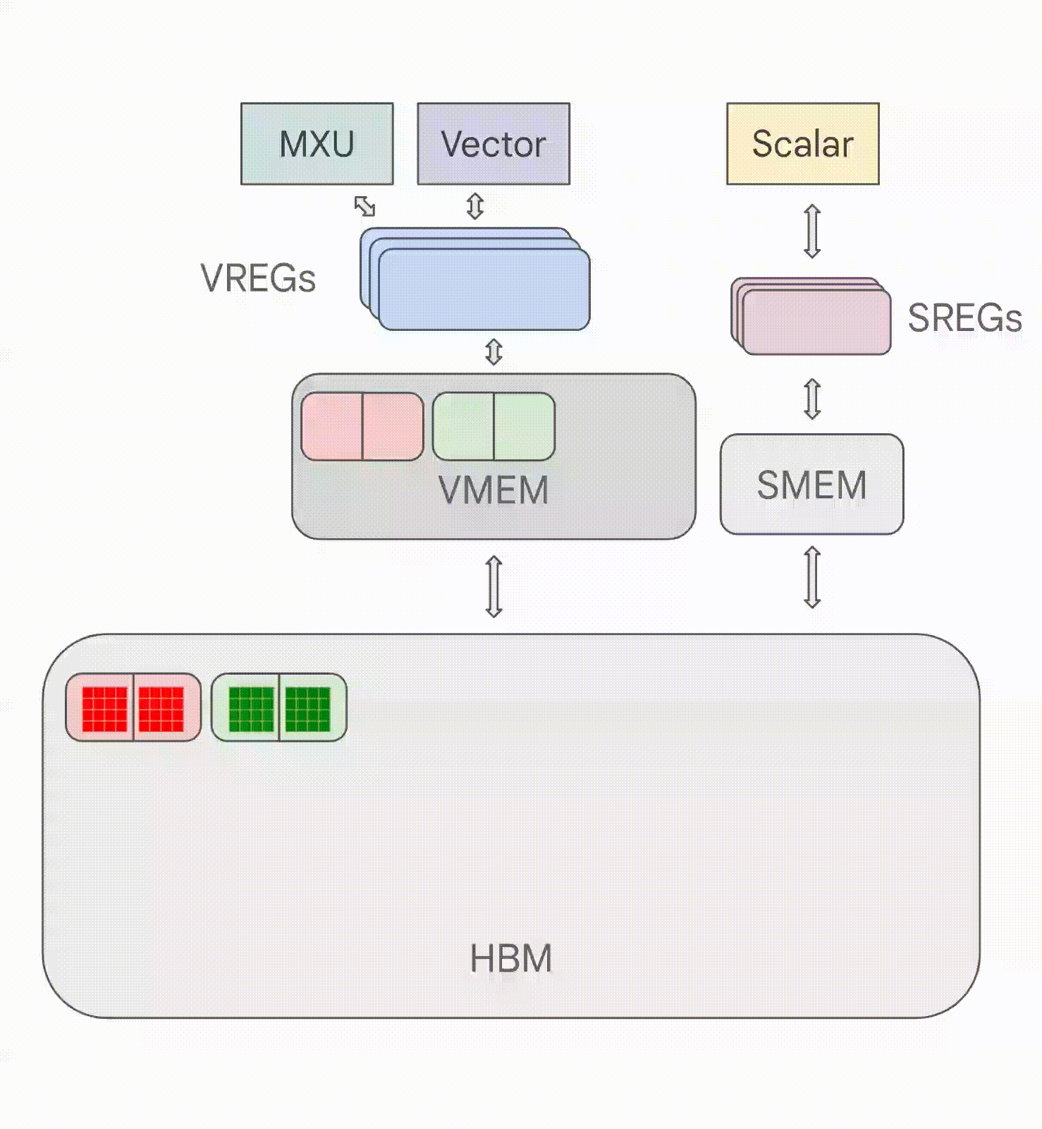
1. Matrix Multiply Unit (MXU)
- - This is the key component of the TensorCore and is a 128x128 systolic array.
- - We'll cover systolic arrays below.
2. Vector Unit (VPU)
- - General elementwise operations (e.g. ReLU, pointwise add/mul, reductions)
3. Vector Memory (VMEM; 32MiB)
- - Memory buffer. Data from HBM is copied into the VMEM before the TensorCore can do any computations.
4. Scalar Unit + Scalar Memory (SMEM; 10MiB)
- - Tell the VPU and MXU what to do.
- - Manages control flow, scalar operations, and memory address generation.
If you're coming from NVIDIA GPUs, there's some initial observations that might throw you off:
- On-chip memory units (CMEM, VMEM, SMEM) on TPUs are much larger than L1, L2 caches on GPUs.
- HBM on TPUs are also much smaller than HBM on GPUs.
- There seems to be a lot less "cores" responsible for the computation.
This is the complete opposite of GPUs where they have smaller L1, L2 caches (256KB and 50MB, respectively for H100), larger HBM (80GB for H100), and tens of thousands of cores.
Before we go any further, recall that TPUs are capable of extremely high throughput just like GPUs. TPU v5p can achieve 500 TFLOPs/sec per chip and with a full pod of 8960 chips we can achieve approximately 4.45 ExaFLOPs/sec. The newest "Ironwood" TPUv7 is said to reach up to 42.5 ExaFLOPS/sec per pod (9216 chips).
To understand how TPUs achieve this, we need to understand their design philosophy.
TPU Design Philosophy
TPUs achieve amazing throughput and energy efficiency by relying on two large pillars and a key assumption: systolic arrays + pipelining, Ahead-of-Time (AoT) compilation, and the assumption that most operations can be expressed in a way that maps well to systolic arrays. Fortunately, in our modern DL era, matmuls comprise the bulk of computation, which are fit for systolic arrays.
TPU Design choice #1: Systolic Arrays + Pipelining
Q. What is a Systolic Array?
Systolic array is a hardware design architecture consisting of a grid of interconnected processing elements (PE). Each PE performs a small computation (e.g. multiply and accumulate) and passes the results to neighboring PEs.
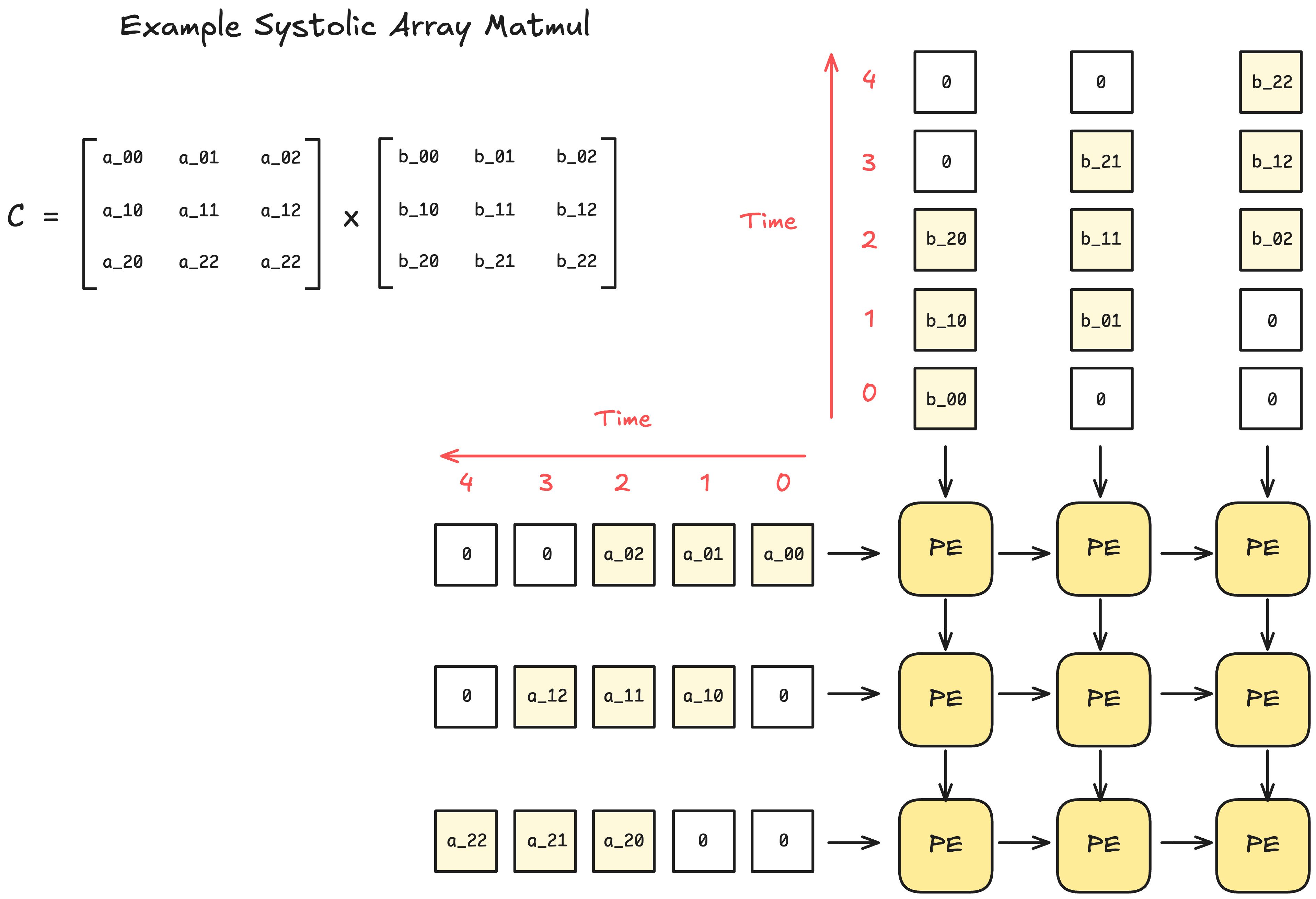
The benefit of such a design is that once data is passed into a systolic array, additional control logic on how data should be processed is not required. Also, when given a large enough systolic array, there's no memory read/writes other than the input and output.
Due to their rigid organization, systolic arrays can only handle operations with fixed dataflow patterns, but fortunately matrix multiplication and convolutions fit perfectly in this regime.
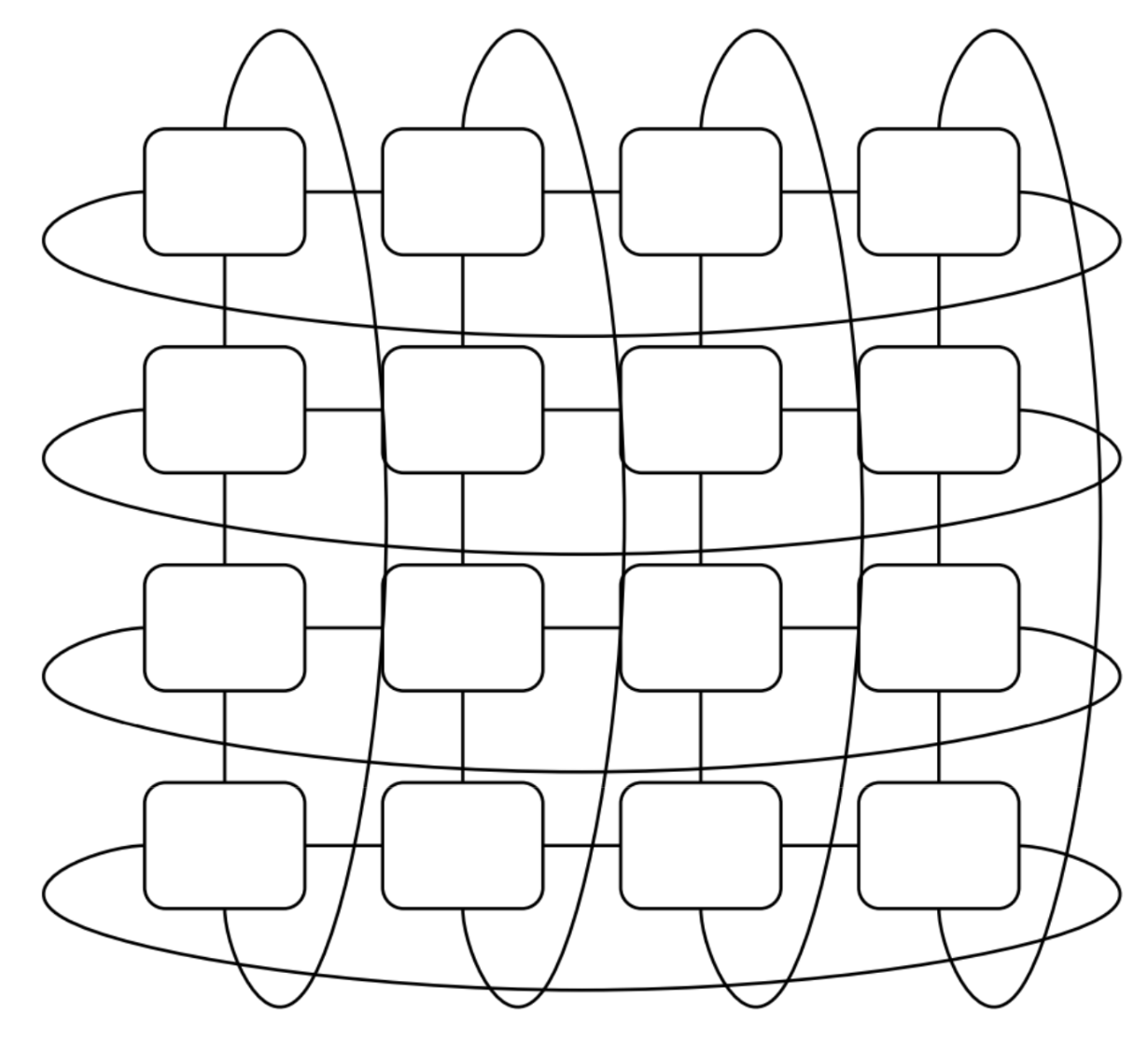
Moreover, there's clear opportunities for pipelining to overlap computation with data movements. Here's a diagram below for a pipelined pointwise operation on a TPU.
Aside: Downsides of Systolic Arrays - Sparsity
You can see how systolic arrays love dense matrices (i.e. When every PE is active nearly every cycle). However, the downside is that there's no performance improvements for sparse matrices of the same size: the same number of cycles will have to be performed where PEs are still doing work even for zero-valued elements.
Dealing with this systematic limitation of systolic arrays will become more important if the DL community favors more irregular sparsity (e.g. MoE).
TPU Design choice #2: Ahead of Time (AoT) Compilation + Less Reliance on Caches
This section answers how TPUs achieve high energy efficiencies through avoiding caches through hardware-software codesign of TPUs + XLA compiler.
First, recall that traditional caches are designed to handle unpredictable memory access patterns. A program for one application can have vastly different memory access patterns with those from programs for other applications. In essence, caches allow hardware to be flexible and adapt to a wide range of applications. This is a large reason why GPUs are very flexible hardware (note: compared to TPUs).
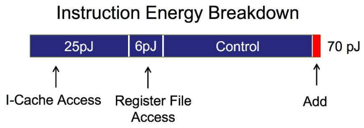
However, cache accesses (and memory accesses in general) cost significant energy. Below is a rough estimate of energy costs for operations on a chip (45nm, 0.9V; [18]). The key takeaway here is that memory access and control takes up most of our energy and that arithmetic takes up significantly less.
But what if your application is very specific and its computation/memory access patterns are highly predictable?
As an extreme example, if our compiler can figure out all the required memory accesses ahead of time, then our hardware can get by with just a scratchpad memory as a buffer with no caches.
This is what the TPU philosophy aims for and exactly why TPUs were codesigned with the XLA compiler to achieve this. The XLA compiler generates optimized programs by analyzing computation graphs ahead of time.
Q. But JAX also works well with TPUs, but they use @jit?
JAX+XLA on TPUs are in a hybrid space of JIT and AOT, thus the confusion. When we call a jitted function in JAX for the first time, JAX traces it to create a static computation graph. This is passed to the XLA compiler, where it is turned into a fully static binary for TPUs. It is during the last conversion stage where TPU-specific optimizations are done (e.g. minimize memory accesses) to tailor the process to TPUs.
But there's one caution: jitted functions have to be compiled and cached again if they are run with different input shapes. That's why JAX does poorly with any dynamic padding or layers with for loops with different lengths that depend on the input.
Of course, this approach sounds very good but there are also inconvenient downsides. There's the lack of flexibility and this heavy reliance on compilers is a double-edged sword.
But why did Google still pursue this design philosophy?
TPUs and Energy Efficiency (TPUv4)
The previous diagram for energy usage was not an accurate representation for TPUs, so here's the energy usage breakdown for TPUv4. Note that TPUv4 is 7nm and the 45nm is there for a comparison ([3], [16]).
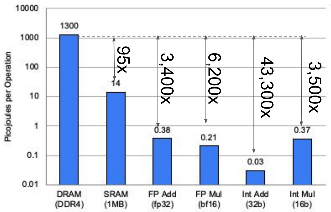
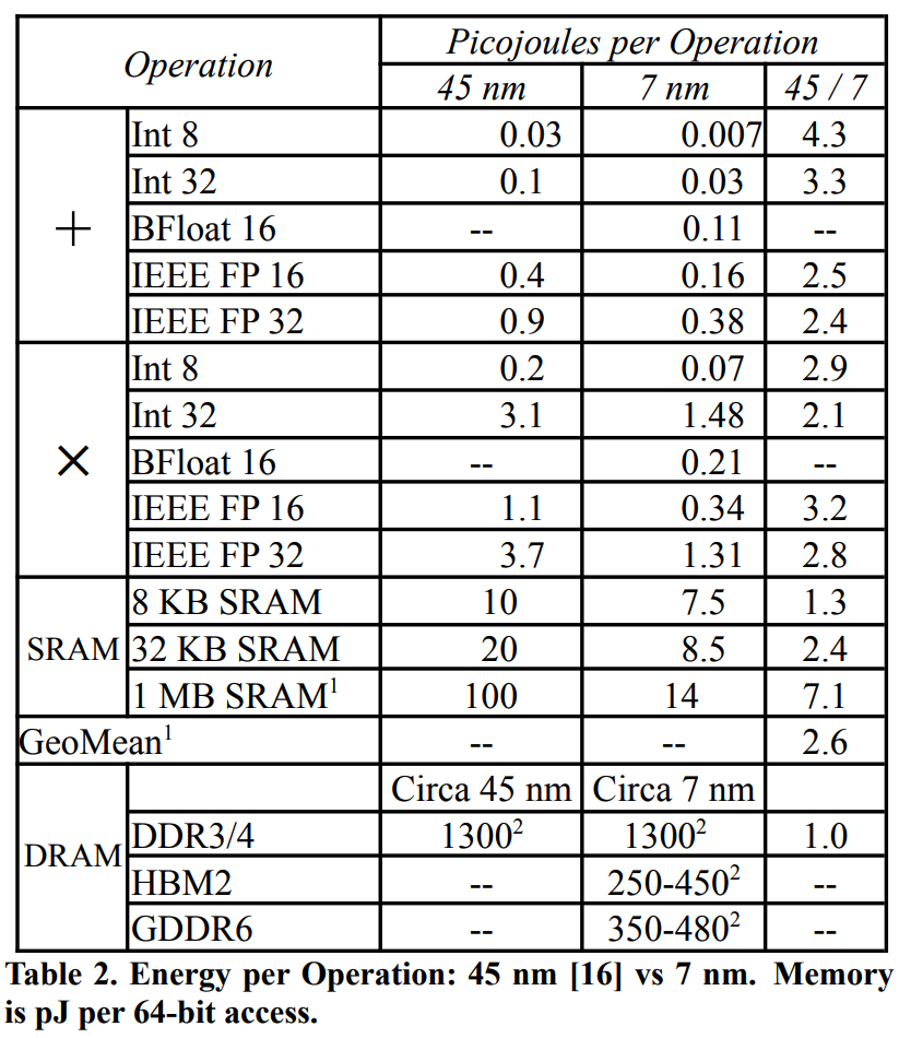
The bar plot on the left shows us the visualization of values, but one thing to note is that modern chips use HBM3, which uses much less energy than DDR3/4 DRAM shown over here. Nevertheless, this shows how memory operations consume a couple orders of magnitudes more energy.
This is a good connection with modern scaling laws: we're very much happy to increase FLOPS in exchange for reduced memory operations. So reducing memory operations has double the optimization benefits since they not only make programs fast, but also consume much less energy.
TPU Multi-Chip Level
Let's move up the ladder to look at how TPUs work in multi-chip settings.
Tray Level (a.k.a "Board"; 4 chips)
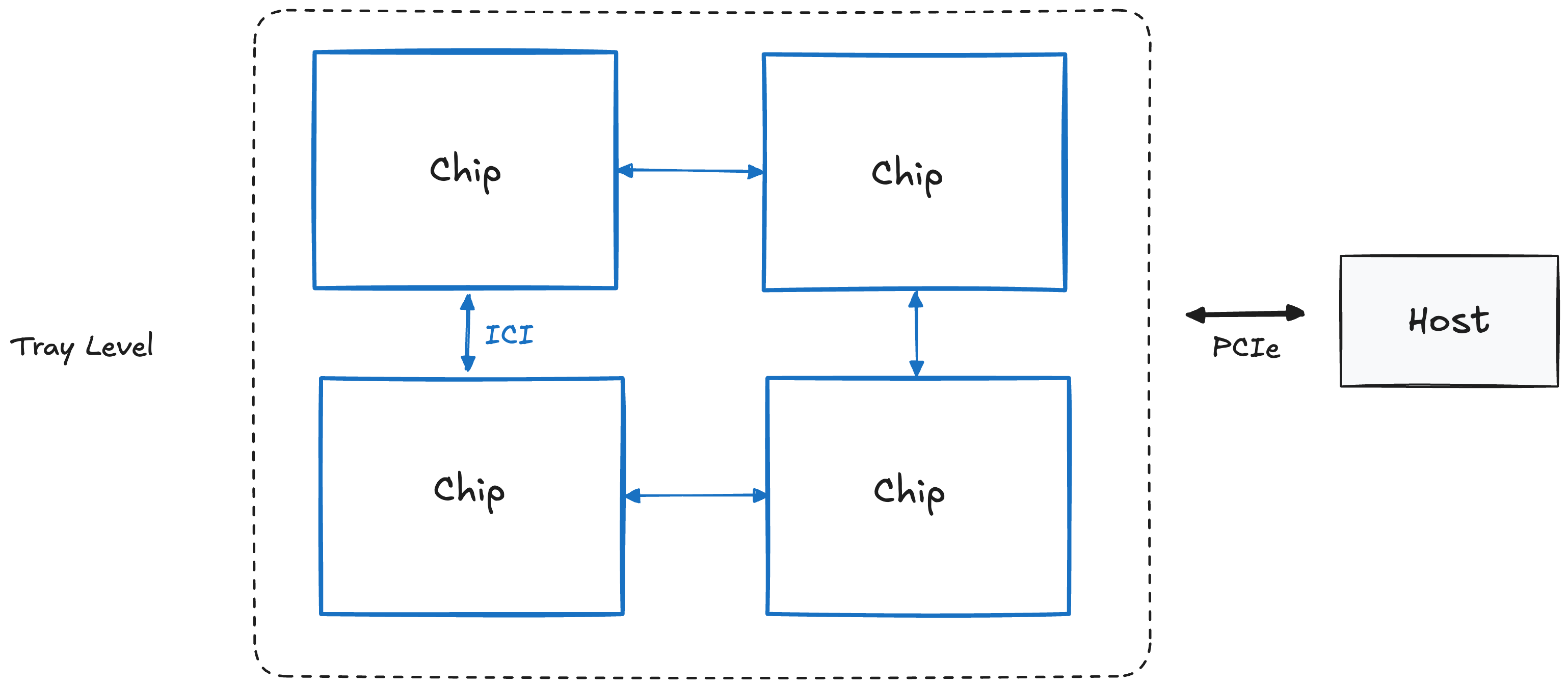
A single TPU tray consists of 4 TPU chips or 8 TensorCores (referred to as just "cores"). And each tray gets its own CPU Host (Note: For inference TPUs, one host accesses 2 trays since they only have 1 core per chip).
Host⇔Chip connection is PCIe, but Chip⇔Chip connection is Inter-Core Interconnect (ICI), which has a higher bandwidth.
But ICI connections extend much further to multiple trays. And for this, we need to move up to the Rack level.
Rack Level (4x4x4 chips)
The especially exciting part about TPUs is in their scalability, which we start to see from the Rack level.
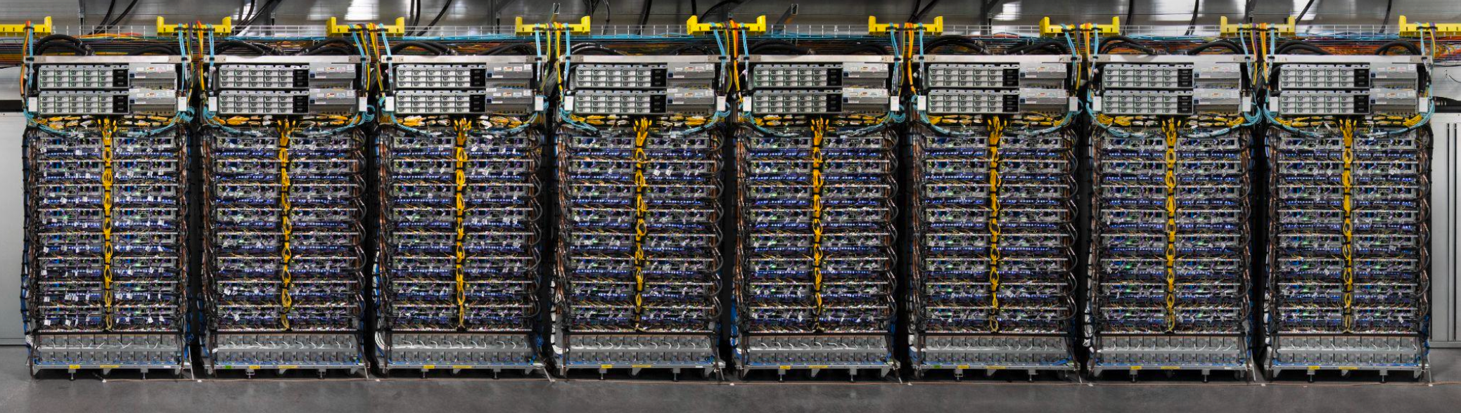
A TPU rack consists of 64 TPUs that are connected in a 4x4x4 3D torus. If you saw Google's promotion material for TPUs like below, this is an image of 8 TPU racks.
But before we dive into racks, we need to clarify some confusing terminology: racks vs pods vs slices.
Q. What's the difference between a "TPU Rack" vs a "TPU Pod" vs "TPU Slice?
Different Google sources use them a bit differently and sometimes use "TPU Pods" and "TPU Slices" interchangeably. But for this article we'll stick with the definitions used in Google's TPU papers and in GCP's TPU documentation ([3], [7], [9]).
- TPU Rack:
- - Physical unit that contains 64 chips. Also known as a "cube".
- TPU Pod:
- - Maximum unit of TPUs that can be connected through ICI and optical fibers.
- - Also known as a "Superpod" or "Full pod". For example, a TPU Pod for TPUv4 would consist of 4096 chips or 64 TPU Racks.
- TPU Slice:
- - Any configuration of TPUs that are in between 4 chips and the Superpod size.
The key difference is that a TPU Rack and a TPU Pod is a physical unit of measure whereas a TPU Slice is an abstract one. There's, of course, important physical properties for setting a TPU Slice but let's abstract this away for now.
For now, we'll work with physical units of measure: TPU Racks and TPU Pods. This is because seeing how TPU systems are physically wired together allows us to understand TPU design philosophies better.
Now back to TPU racks (for TPUv4):
A single TPU Rack consists of 64 chips that are connected together through ICI and Optical Circuit Switching (OCS). In essence, we connect multiple trays together to emulate a system of 64 chips. This theme of putting together smaller parts to make a supercomputer continues to appear later.
Below is a diagram for a single TPUv4 Rack. It's a 4x4x4 3D torus where each node is a chip, and the arrows in blue are ICI while the lines on the faces are OCS (redrawn from [7]).
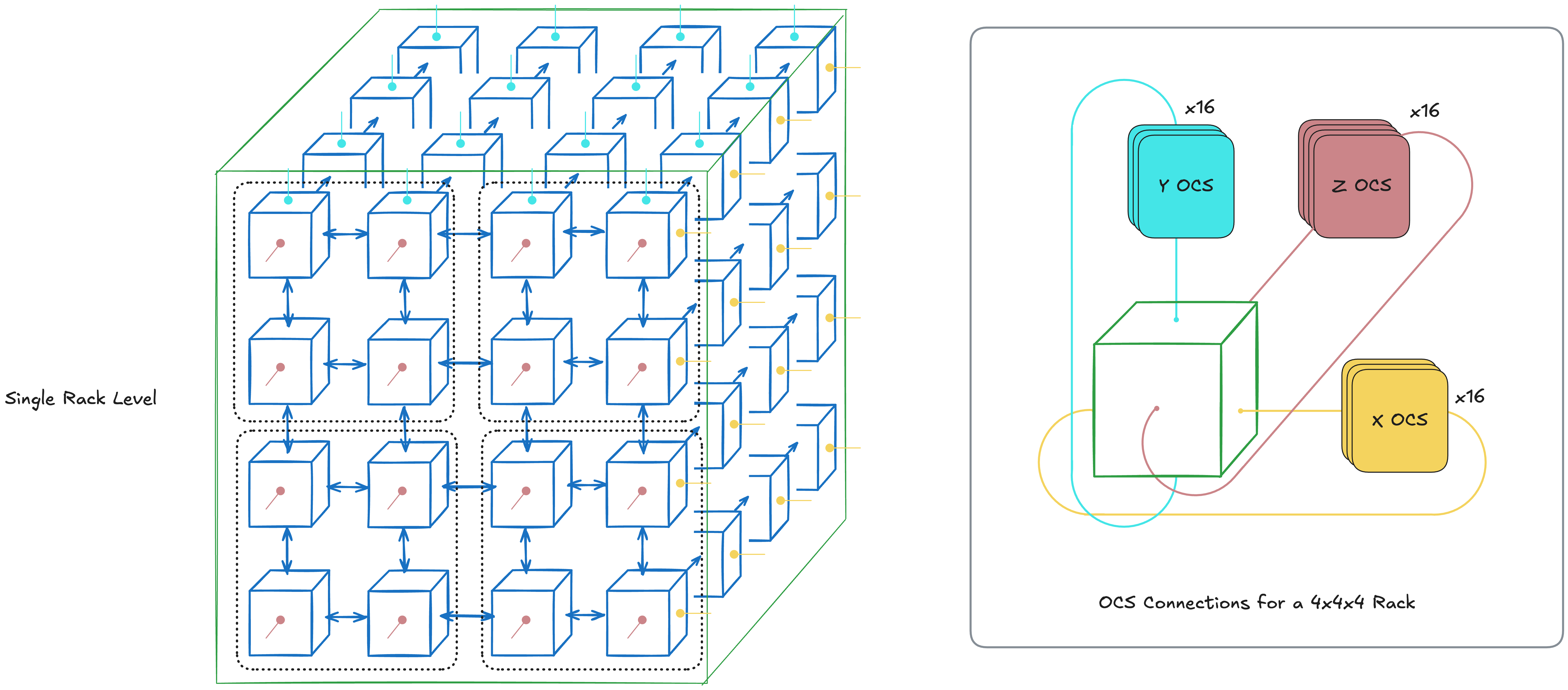
This diagram, however, raises a couple questions. Why is the OCS only used for the faces? In other words, what are the benefits of using OCS? There's 3 large benefits and we'll cover the other two down below later.
Benefits of OCS #1: Wraparound
Faster communication between nodes through wraparound
The OCS also acts as a wraparound for a given TPU configuration. This reduces the worst case number of hops between two nodes from N-1 hops to (N-1)/2 per axis, as each axis becomes a ring (1D torus).
This effect becomes more important as we scale up further since reducing chip-to-chip communication latency becomes crucial for high parallelization.
Aside: Not all TPUs have 3D Torus Topologies
Note: older TPU generations (e.g. TPUv2, v3) and inference TPUs (e.g. TPUv5e, TPUv6e) have a 2D torus topology instead of a 3D torus like below. The TPUv7 "Ironwood", however, seems to be a 3D torus although it's promoted as an inference chip (Note: I'm only assuming from their promotional material).
Full Pod Level (aka "Superpod"; 4096 chips for TPUv4)
Just like how we connected multiple chips together to make a TPU Rack, we can connect multiple racks to make one large Superpod.
A Superpod also refers to the largest configuration of interconnected chips (using only ICI and OCS) that TPUs can reach. There is a multi-pod level next, but this has to go through a slower interconnect and we'll cover this after this.
This changes depending on the generation, but for TPUv4 is 4096 chips (i.e. 64 Racks of 4x4x4 chips). For the newest TPUv7 "Ironwood", this is 9216 chips.
The diagram below shows one Superpod for TPUv4.
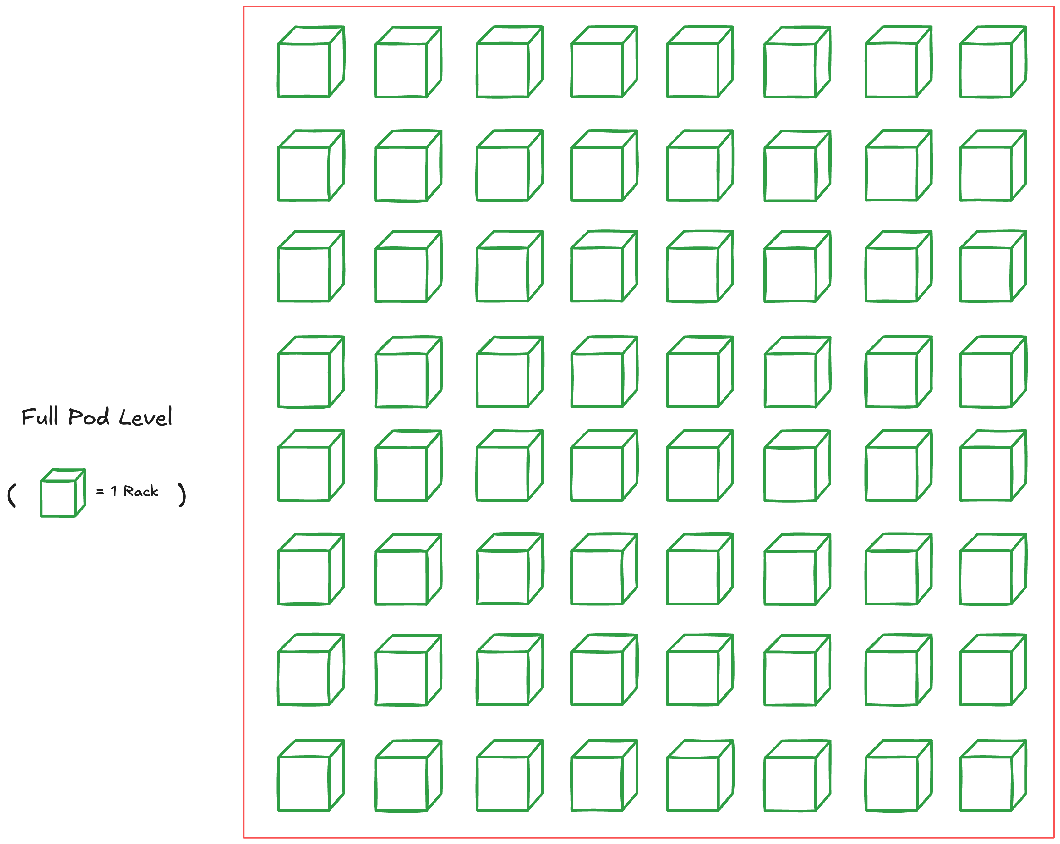
Note how each cube (i.e. a TPU Rack) is connected with each other through OCS. This also allows us to take slices of TPUs in a pod.
TPU Slices with OCS
We can request subsets of TPUs within the pod and these are TPU Slices. But there's multiple topologies to choose from even if you want N chips.
For example, say you want a total of 512 chips. You can ask for a cube (8x8x8), a cigar shape (4x4x32), or a rectangle (4x8x16). Choosing the topology of the slice is a hyperparameter in itself.
The topology you choose will affect the communication bandwidth between nodes. And this directly affects the performance of different parallelism methods.
For example, a cube (ex. 8x8x8) would be preferred for all-to-all communications, such as data parallelism or tensor parallelism, because it has the highest bisection bandwidth. However, a cigar shape (ex. 4x4x32) would be better for pipeline parallelism as it can communicate with sequential layers faster (assuming one layer fits in a sub-slice of 4x4 chips).
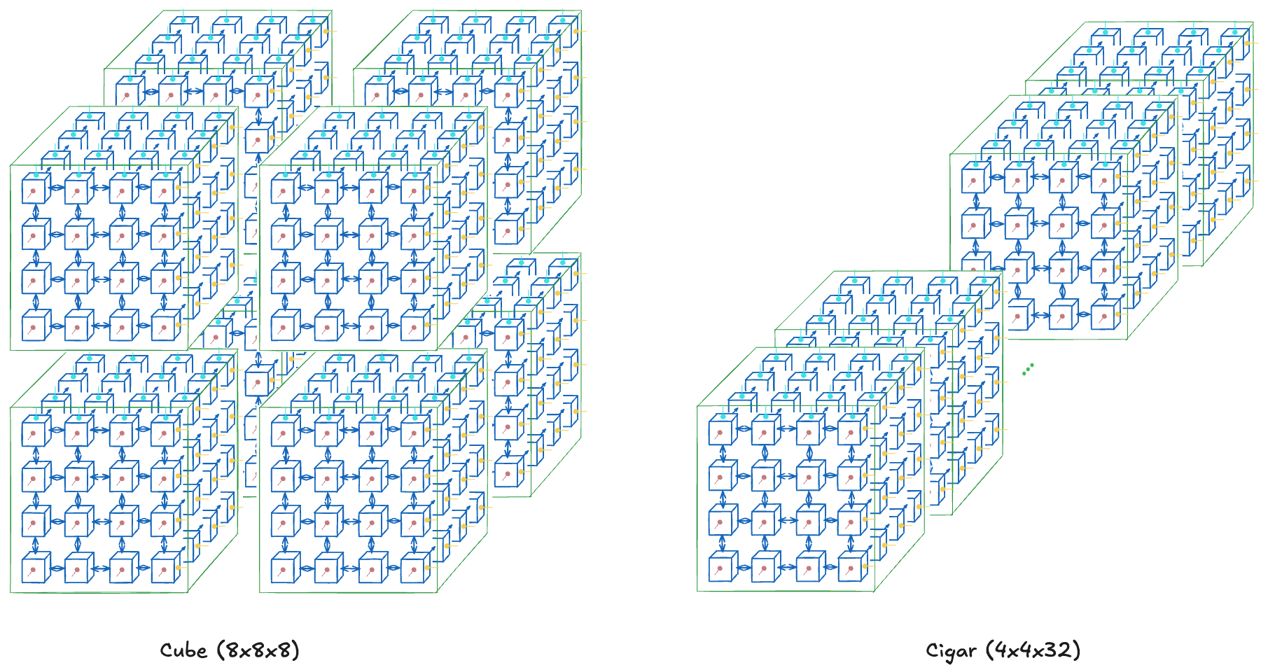
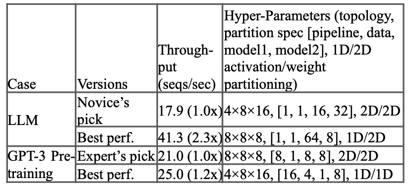
But, of course, optimal topologies would depend on the model and finding this is a job in itself as well. The TPUv4 paper[9] also measured this to show how topology changes can accelerate throughput (Note: I'm not sure which LLM architecture the first row is referring to as it wasn't specified).
We covered TPU Slices, but there's one important feature that contributes to a high operational stability of TPUs.
It's that these slices do not have to be contiguous racks thanks to OCS. This is the second benefit of using OCS–and probably the largest–that we didn't get to earlier.
Benefits of OCS #2: (Reconfigurable) Noncontiguous Multi-Node Slices
Note that this is different from hard-wiring multiple nodes together to emulate noncontiguous slices. Since OCS is a switch instead of being hard-wired, there's much less physical wires across nodes, thus allowing for higher scalability (i.e. larger TPU Pod sizes).
This allows flexible node configuration as scale. For example, say there are three jobs we want to run on a single pod. Although naive scheduling would not allow this, OCS connections instead allow us to abstract away the position of nodes and view the entire pod as just a "bag of nodes" (redrawn from [6]).
This increases pod utilization and possibly much easier maintenance in case of failed nodes. Google described this as "Dead nodes have small blast radius." However, I'm not sure how its liquid cooling would be impacted when only certain nodes have to be shut down.
Finally, there's an interesting extension of this flexible OCS: we can also change the topology of TPU Slices, such as from a regular torus to a twisted torus.
Benefits of OCS #3: Twisted TPU Topologies
We previously saw how we could achieve different TPU Slice topologies by changing (x,y,z) dimensions for a fixed number of chips. This time, however, we'll be working with fixed (x,y,z) dimensions, but instead change how they are wired together to achieve different topologies.
A notable example is going from a regular torus of a cigar shape into a twisted cigar torus as seen below.
The twisted torus case allows for faster communication between chips across the twisted 2D plane. This is especially useful for accelerating all-to-all communications.
Let's dive a little deeper and imagine a concrete scenario where this would help.
Accelerated Training using Twisted Torus
Theoretically, twisting the torus will bring the largest benefit for tensor parallel (TP) since there are multiple all-gather and reduce-scatter operations per layer. It could bring moderate benefits for data parallel (DP) since there's an all-reduce per training step as well, but this would be less frequent.
Imagine we're training a standard decoder-only transformer and we want to employ lots of parallelism to accelerate training. We'll see two scenarios below.
Scenario #1: 4x4x16 Topology (TP + PP; Total 256 chips)
Our z axis will be our pipeline parallel(PP) dimension and our 2D TP dimension will be 4x4. In essence, assume each layer k lies at z=k and that each layer is sharded across 16 chips. Assume standard OCS connections (i.e. nearest-neighbor) if not explicitly drawn.
We'll twist the 2D torus at each z=k, which makes communication between chips in each TP layer faster. Twisting along our PP dimension is unnecessary as they rely mostly on point-to-point communication.
Note: In reality, twisting the torus brings benefits when the number of chips is larger than 4x4. We're using 4x4 only for visualization purposes.
Scenario #2: 16x4x16 Topology (DP + TP + PP; Total 1024 chips)
As an extension, we'll be adding a DP dimension of 4 to our previous scenario. This means there's 4 of scenario #1 models along the x axis.
Notice how twisting the torus is limited to each TP dimension of each DP model (i.e. A 4x4 2D plane for each z=k given k=1…16). There is only a wraparound for the DP dimension so that each row becomes a horizontal ring of size 16.
You might have noticed that there's an alternative topology of 8x8x16 instead (i.e. 2x2 DP dimension), but this becomes more complicated as we're mixing our DP and TP dimensions. Specifically, it's unclear how we should construct the OCS wraparounds for the y-axis while accommodating twisted toruses for each TP dimension.
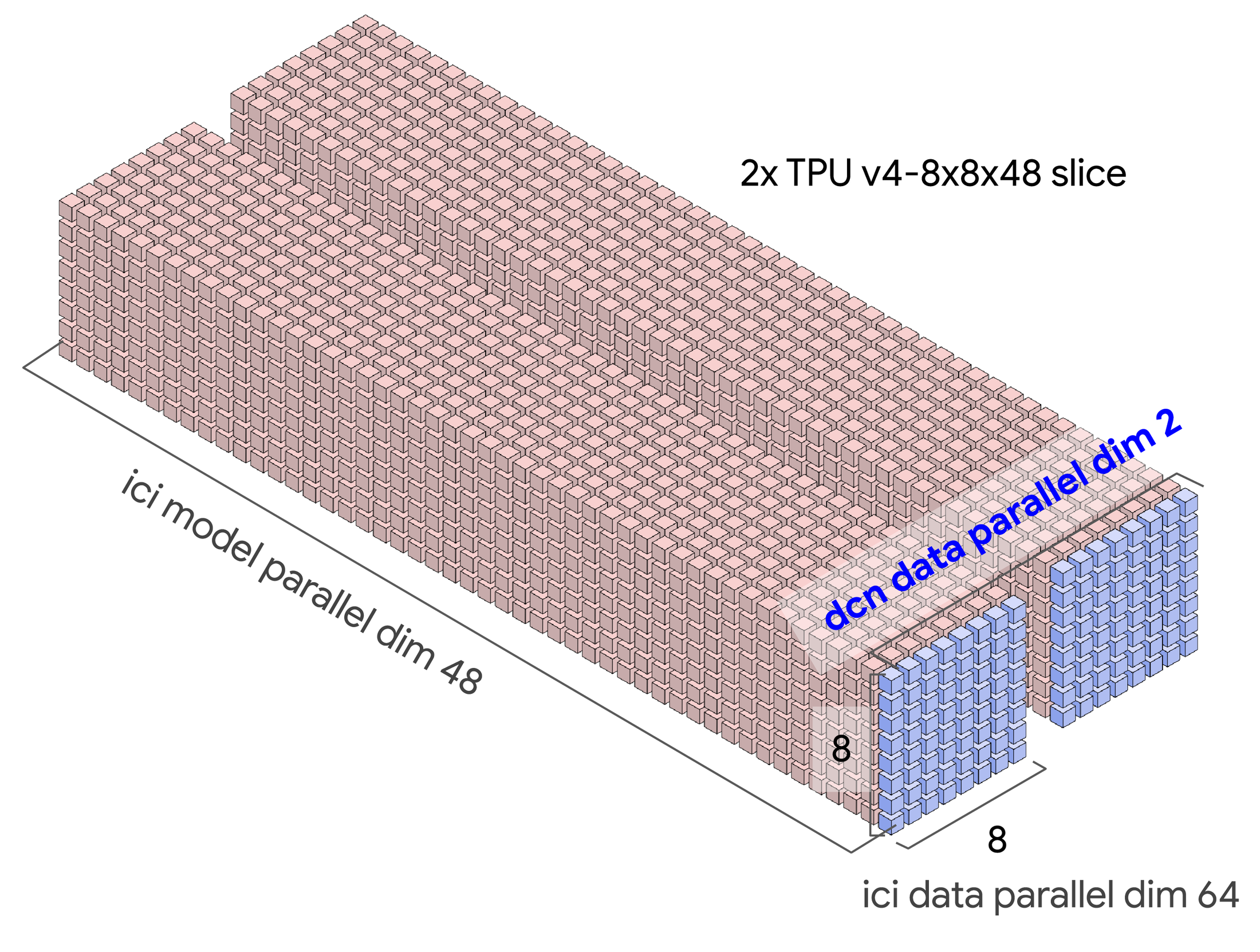
Multi-Pod Level (a.k.a "Multislice"; 4096+ chips for TPUv4)
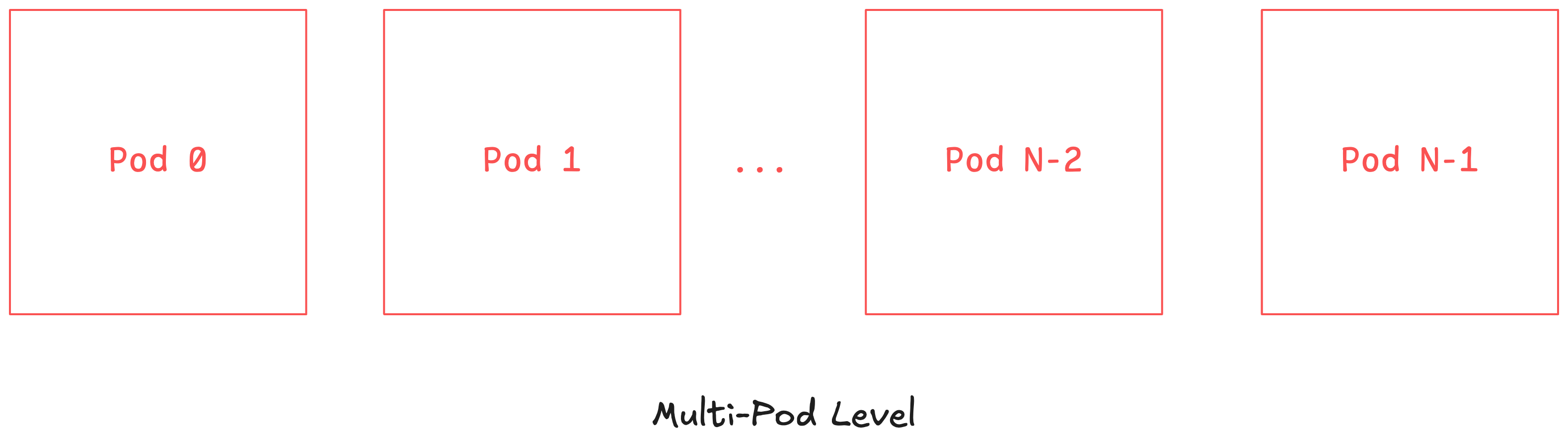
The final level of TPU hierarchy is the Multi-pod level. This is where you can treat multiple pods as one large machine. However, the communication between pods is done through Data-Center Network (DCN), which has a lower bandwidth than ICI.
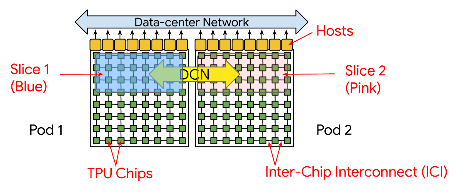
Diagram showing how Multi-pod training can be configured
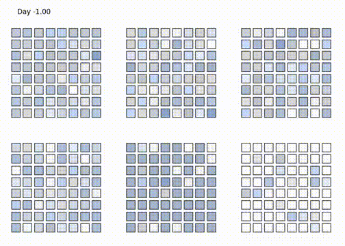
This was how PaLM was trained. It took 56 days to train over 6144 TPUv4s (2 pods). Below you can see the TPU job assignments over 6 pods: green is for PaLM, red is no assignment, and the rest are other jobs. Note that each square is a 4x4x4 cube of TPUs.
Making this possible is difficult on its own, but what makes this more impressive is the focus on developer experience. Specifically, it's about focusing on the question of "How can we abstract the systems/HW part of model scaling as much as possible?".
Google's answer is to make the XLA compiler responsible for coordinating communication between chips at large scales. With the right flags given by researchers (i.e. Parallelism dimensions for DP, FSDP, TP, num slices, etc), the XLA compiler inserts the right hierarchical collectives for the TPU topology at hand (Xu et al, 2021: GSPMD [2]). The goal is to make large scale training happen with as little code changes as possible.
For example, here's a breakdown of an all-reduce operation across multiple slices from Google's blog [1].
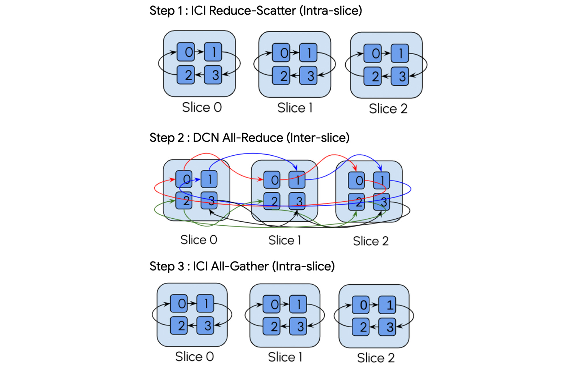
This is to show that the XLA compiler takes care of communication collectives both between slices and within slices.
For a concrete example, there could be a TPU topology like below for training a model. The activation communication happens within a slice through ICI whereas gradient communications will happen across slices through DCN (i.e. across the DCN DP dim) [1].
Putting diagrams to perspective in real-life
I find it helpful to put diagrams into perspective when you have actual photos of hardware. Here's a summary below.
If you’ve seen pictures of Google’s promotion material for TPUs, you might have come across this image below.
This is 8xTPU Pods where each unit is a 4x4x4 3D torus we saw above. Each row in a pod has 2 trays, meaning there's 8 TPU chips per row.
Here’s a single TPUv4 tray:
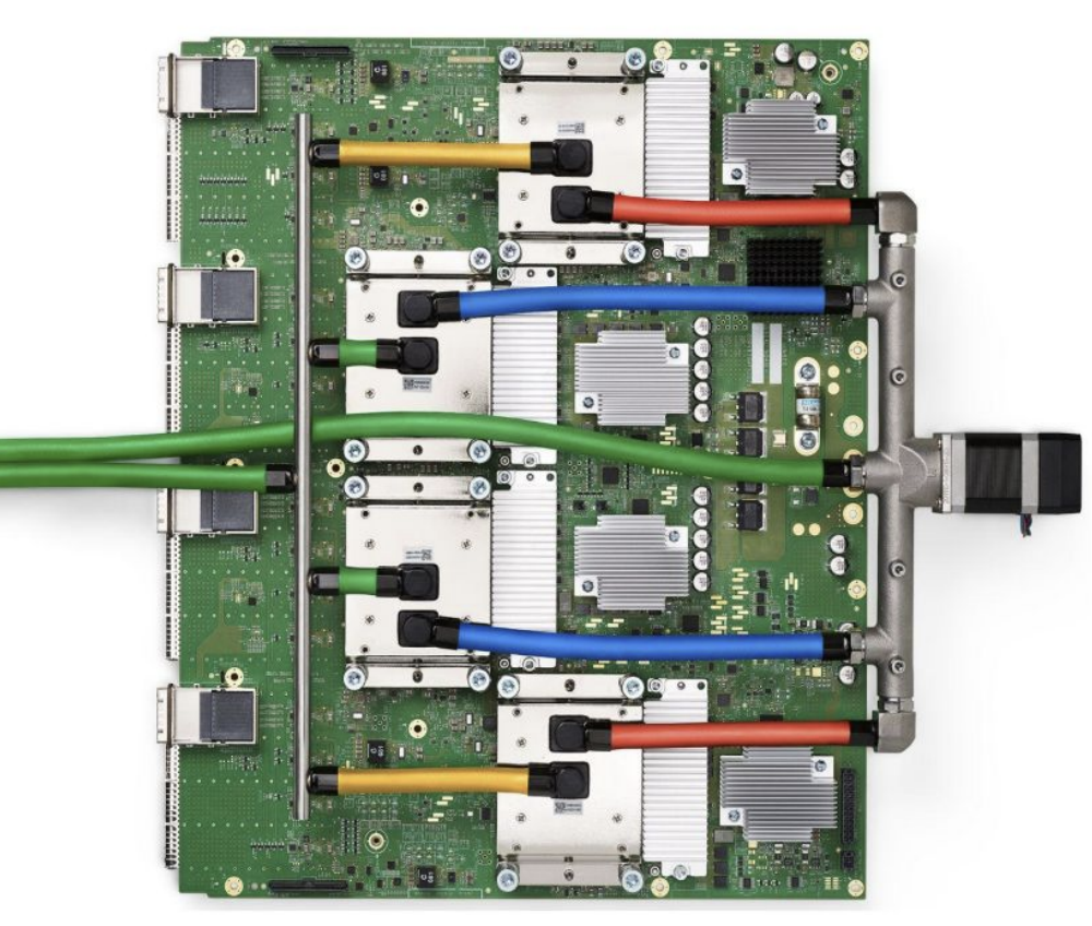
Note that the diagram is simplified to just one PCIe port, but on the actual tray there’s 4 PCIe ports(on the left)--one for each TPU.
And here’s a single chip below:
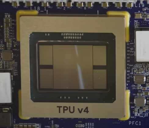
The center piece is the ASIC and the surrounding 4 blocks are the HBM stacks. This is a TPU v4 we’re seeing, so it has 2 TensorCores inside, hence the total of 4 HBM stacks.
I couldn’t find the chip floorplan for TPUv4, so here’s one for TPUv4i which is similar except that it only has 1 TensorCore since it’s an inference chip [3].
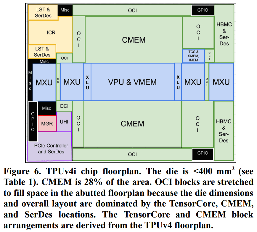
Notice how the CMEM takes up quite some space on the layout for TPUv4i.
Acknowledgements
Thank you to the Google TPU Research Cloud(TRC) for the TPU support!
References
[1] Google Blog: TPU Multi-Slice Trainng
[2] Xu, et al. "GSPMD: General and Scalable Parallelizaton for ML Computation Graphs"
[3] Jouppi et al. "Ten Lessons From Three Generations Shaped Google's TPUv4i"
[4] How to Scale Your Model - TPUs
[5] Domain Specific Architectures for AI Inference - TPUs
[8] Jouppi et al. "In-Datacenter Performance Analysis of a Tensor Processing Unit" -- TPU origins paper
[9] Jouppi et al. "TPU v4"-- TPUv4 paper
[10] PaLM training video
[11] HotChips 2021: "Challenges in large scale training of Giant Transformers on Google TPU machines"
[12] HotChips 2020: "Exploring Limits of ML Training on Google TPUs"
[14] HotChips 2019: "Cloud TPU: Codesigning Architecture and Infrastructure"
[15] ETH Zurich's Comp Arch Lecture 28: Systolic Array Architectures
[17] Camara et al. "Twisted Torus Topologies for Enhanced Interconnection Networks."
[18] Horowitz article: "Computing's Energy Problem(and what we can do about it)"
What's Your Reaction?
 Like
0
Like
0
 Dislike
0
Dislike
0
 Love
0
Love
0
 Funny
0
Funny
0
 Angry
0
Angry
0
 Sad
0
Sad
0
 Wow
0
Wow
0