


More than you wanted to know about how Game Boy cartridges work
More than you wanted to know about how Game Boy cartridges work
I set out a while ago to make a Game Boy cartridge from scratch. This is not a novel goal; bootleg Game Boy cartridges have existed almost as long as the Game Boy itself has, and there are many third-party cartridges now available for purchase, or that have copyleft designs.
But I wanted to know how Game Boy cartridges work. I was also excited to use the PIO functionality of the RP2040 microcontroller. Now, after a few years (!) of research and design, I have made my design for a bootleg Game Boy cartridge available for everyone to use. In this post, I’m going to take you through everything I learned along the way.
I will be quick to note that this document doesn’t contain any new research! Instead, it’s my attempt to gather together information relevant to making custom Game Boy cartridges in one place, and present that information in a way that is easy to digest for people who start off with about the same level of knowledge I started with when I first dipped my toes into the Game Boy cartridge pool.
Please let me know if you find any errors or have questions!
Prerequisites
I’m going to assume that you have some knowledge of how digital memory works, e.g., that you know what a “byte” is and broadly how processors address memory. (If you don’t have this knowledge but you’re curious and want to get up to speed, I recommend Sebastian Lague’s “Exploring How Computers Work” series, or this chapter on Digital Memory Terms and Concepts from All About Circuits.) I’m also going to assume that you have enough knowledge of computer internals to know what a microprocessor is, and how a microprocessor might communicate with other electronic components. You should have some understanding of hexadecimal and binary numbers. However, you don’t need to know anything in particular about electronics or electronic components.
Rodrigo Copetti’s Game Boy/Game Boy Color Architecture: A Practical Analysis is a good general overview of the Game Boy hardware, and is also worth a read, to familiarize yourself with Game Boy components and terminology.
Conventions, notations and caveats
In this document, I’ll write hexadecimal numbers with a preceding
0x (e.g., 0xABCD) and binary numbers with a
preceding 0b (e.g., 0b10100101). If the name
of a pin or connection is preceded by an underscore (_),
that means that the pin is active low (i.e., the functionality
indicated by the pin is active when the pin is at zero volts).
You’ll find the occasional paragraph marked with “💡” in the margin. These are technical asides: snippets of facts and explanations that I wanted to include, but aren’t necessary to understand the overall content of the document. Feel free to skip!
Also, please note that when I’m describing what some IC “does” in this document, I’m attempting to describe its behavior, not how it works internally. There have been some impressive efforts (e.g., the audio amplifier chip, CPU and MBC1, DMG SoC) to examine the actual silicon of some common Game Boy components, but a lot of what is known about the Game Boy still comes from developer documentation and empirical observation.
When I discuss technical specifics of the “Game Boy CPU” in this document, I’m referring specifically to the system-on-chip (SoC) of the original Game Boy (commonly referred to as the “DMG”). While there are many technical differences between the Game Boy-compatible platforms (DMG, Game Boy Pocket, Game Boy Color, and the backwards compatibility mode of the Game Boy Advance and Game Boy Advance SP), they all interact with cartridges in a similar way. The broad outlines of what I describe in this document should be applicable to all of these platforms.
What makes the Game Boy special?
First, let’s discuss the reason we’re even doing any of this in the first place, because it might not be obvious. Why bother to do weird stuff with the Game Boy anyway?
I don’t think it’s unfair to characterize a lot of retro gaming enthusiasm as being rooted in nostalgia. And, y’know, there’s nothing wrong with nostalgia! But I never owned a Game Boy as a kid (my formative scene was BBS doors and DOS shareware), and though I love hearing others’ memories of (e.g.) meeting MissingNo after bedtime, I have no such memories of my own. I’m interested in the Game Boy for a number of other reasons, such as:
- The Game Boy is a relatively powerful machine for its time, but it still has a very simple design that is easy to learn and understand. It’s not too difficult for a programmer or hardware designer to form a more or less complete understanding of the Game Boy’s functioning that they can keep in their head all at once.
- The Game Boy is portable and power-efficient.
- You don’t need to circumvent copy protection or region lockout hardware to write custom software for the Game Boy, since the Game Boy has none.
- The Game Boy is incredibly well documented. There is seemingly no end to community-produced technical documentation about the Game Boy, including detailed hardware schematics.
- The Game Boy has a very extensive software library, including not just the familiar games released during its original commercial run, but a host of independently-produced games created in the meantime. And new Game Boy games are still being released today.
- There are many actively maintained open source toolchains for Game Boy software development, including a C toolchain, a number of different assemblers (including my fave RGBDS), and a visual scripting programming environment. If you want to develop software for the Game Boy, you have a lot of choices.
- There are probably more than 100 million Game Boys out there in the world somewhere. But even if you can’t get your hands on an original console, the Game Boy is easy and cheap to emulate to a fair degree of accuracy, even on meager hardware. There are also multiple FPGA implementations of the Game Boy SoC that are (mostly) compatible with original game cartridges.
In short: the Game Boy, as a platform, is simple, capable, extensible, and low-cost. If the Game Boy didn’t already exist, someone would have to invent it (as a fantasy console, probably).
Game Boy cartridges: The basics
So let’s start talking about Game Boy cartridges.
Here in the 2020s, the boundary between “software” and “hardware” is pretty clear cut. Generally, when you buy a computer (or video game console, or some other computer-like device), that device has an operating system, which you can use to load software from non-volatile storage (like an SSD, or a SD card) into RAM, and then run that software. Sometimes software requires the use of particular peripheral, but the process of loading and running software is more or less totally decoupled from hardware. The program is the same regardless of where you loaded it from. (Even Nintendo Switch “cartridges” are essentially just SD cards.)
But in the late 1980s and early 1990s, the distinction between software and hardware was a bit more blurry, especially when we’re talking about video game consoles and home computers. The Game Boy has a tiny chunk of built-in ROM that serves as a bootloader, but it has no real “operating system.” In fact, it has no built-in rewritable non-volatile storage of any kind. Consequently, you can’t just “load” software “onto” the Game Boy. If you’re a game developer in the 1980s/1990s and you want to distribute a Game Boy game, you have to ship what amounts to a hardware peripheral—a cartridge—that provides the actual memory ICs that the Game Boy will use to run the game. (This is somewhat analogous to shipping a PlayStation 5 game not as a physical Blu-ray disc but as the disc and the drive needed to read it.)
So in a sense, the Game Boy on its own is incomplete. It needs a cartridge in order to function. A benefit of this arrangement is that it’s fairly easy to introduce custom hardware on a cartridge that extends the Game Boy’s functionality (like an accelerometer or a real-time clock). The main drawback of the arrangement is that you’re not just shipping bits; you’re shipping a little piece of computer hardware. And if your hardware doesn’t work properly, the Game Boy just… won’t do anything.
Living on the (cartridge) edge
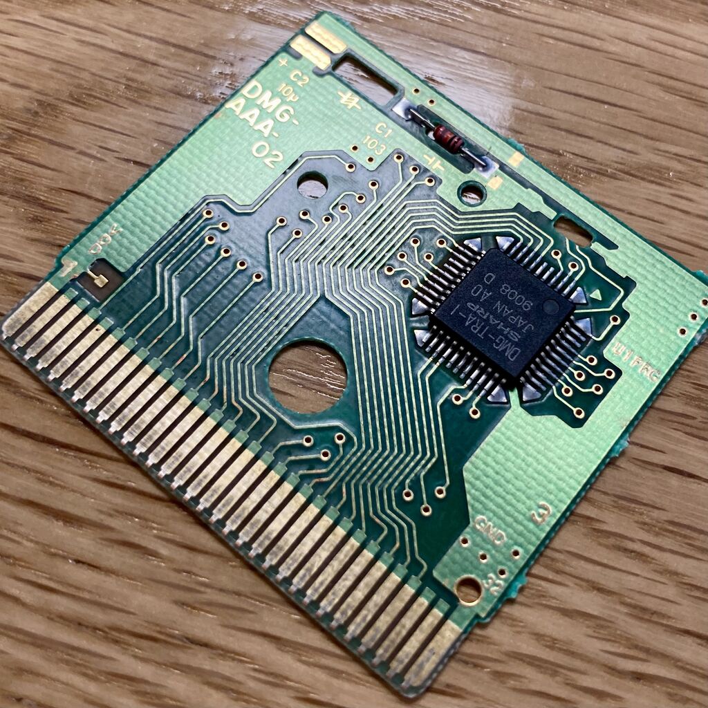
Here’s a photograph of the PCB of a Tetris cartridge, which is about
as simple as a Game Boy cartridge can get:
The exposed gold strips at the bottom of the cartridge are called the “edge connector.” They’re what plug into the cartridge slot on the Game Boy itself. The IC in the upper right-hand corner is a ROM IC, which is connected to the cartridge edge with conductive traces.
The cartridge edge (and the cartridge socket on the Game Boy) has
thirty-two pins, as illustrated in the following diagram:
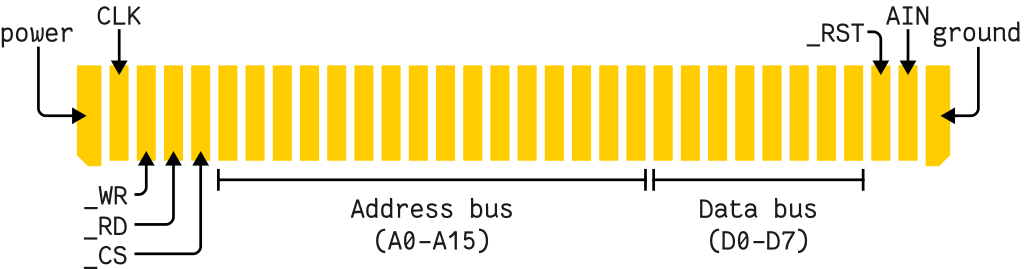
The Game Boy delivers five volts to the cartridge via the power pin;
the ground pin connects to the Game Boy’s ground. A few of the other
pins are not relevant to our purposes here (CLK,
_RST and AIN), so we shall set aside their
mysteries for the time being. The remaining 27 pins can be categorized
like so:
- Flow control pins:
_WR,_RD,_CS(“write,” “read,” “chip select”) - The address bus:
A0–A15(16 bits) - The data bus:
D0–D7(8 bits)
In the simplest possible scenario, here’s what happens between the
Game Boy and the cartridge. When the program running on the Game Boy
wants to read data from the cartridge ROM, the Game Boy sets the
_WR pin high, and the _RD pin low, and writes
the address of the byte that it wants to read onto the address bus. The
ROM chip, recognizing that the _WR pin is low, looks up the
appropriate byte for that address, and then writes the value of that
byte to the data bus. (The whole process begins when you turn the Game
Boy on: the Game Boy is hard-coded to read its first instruction from
memory address 0x0100, which corresponds to a location on
the cartridge ROM chip.)

Get on the bus
When I use the word “bus,” what I mean is “a group of pins that
multiple pieces of hardware are connected to” (usually intended to
transmit data). When I say that a component “writes” a value to the bus,
what I mean is that the component applies either a low voltage or a high
voltage to the pins of the bus, following the digits of the binary
representation of that value. For example, if the Game Boy wants the
value of the byte at address 0x4567, it would set each of
the address pins to be either high (5v) or low (ground), based on the
binary representation of that address, starting from the least
significant bit. The binary representation of 0x4567 is
0b0100010101100111, so A0 would be 1,
A1 would be 1, A2 would be 1, A4
would be zero, etc. On the address bus this would look like:
A15 |
A14 |
A13 |
A12 |
A11 |
A10 |
A9 |
A8 |
A7 |
A6 |
A5 |
A4 |
A3 |
A2 |
A1 |
A0 |
|---|---|---|---|---|---|---|---|---|---|---|---|---|---|---|---|
| 0v | 5v | 0v | 0v | 0v | 5v | 0v | 5v | 0v | 5v | 5v | 0v | 0v | 5v | 5v | 5v |
When the ROM chip writes the value of a byte to the data bus, it
likewise sets the values of the pins according to the binary
representation of that value. So, e.g., the value 0xAB in
binary is 0b10101011. On the data bus this would look
like:
D7 |
D6 |
D5 |
D4 |
D3 |
D2 |
D1 |
D0 |
|---|---|---|---|---|---|---|---|
| 5v | 0v | 5v | 0v | 5v | 0v | 5v | 5v |
For the purposes of this document, “high” and “low” mean the same thing as 1 and 0 (respectively). When I say that a component is “driving” a bus, what I mean is that the component in question is the component that is currently applying voltage (0v or 5v) to that bus.
By the way, this kind of bus—where there is one pin for each bit of the data value and address value—is called a parallel bus. There’s another kind of bus, called a serial bus, where data and addresses are transmitted one bit at a time, and there is an on-wire protocol for determining which bits are addresses and which bits are data. The benefit of a parallel bus is that it can be very fast, since it can transmit multiple bits per clock cycle. Additionally, memory ICs designed for a parallel bus can be less sophisticated electronically than their serial counterparts, because no extra logic is needed to serialize/deserialize data and addresses. The drawback of a parallel bus is that it’s difficult to scale, both in terms of speed and bandwidth. The Game Boy’s 16-bit/8-bit bus running at 4MHz is easy, but getting (say) a working a 64-bit bus running at a couple gigahertz requires some esoteric engineering.
Memories and warfare
Okay. So far we know about the _WR flow control pin, the
address bus, and the data bus. And we know that the Game Boy can read
data from the ROM chip on the cartridge by setting and reading values
from these pins. This is a good start!
Now, if the Game Boy only had one memory chip, then we could
stop the explanation there. But the situation in reality is more
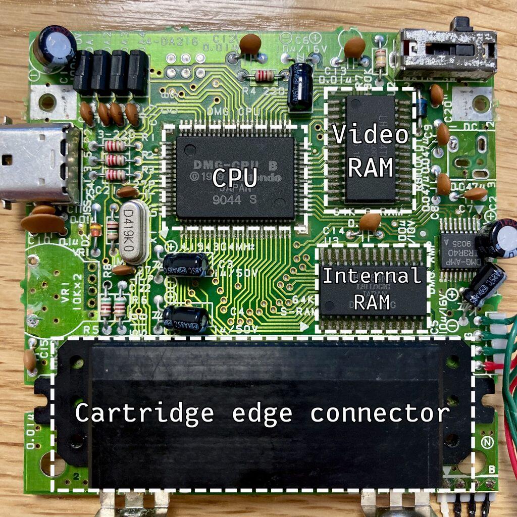
complicated. The image below shows the main board of a Game Boy DMG,
showing the other memory ICs that the Game Boy CPU is connected
to. (The cartridge edge connector is what the cartridge plugs into.)
In fact, the Game Boy can have up to four memory ICs connected to it:
- Internal RAM (“work ram”)
- Video RAM
- ROM on the cartridge (read-only memory; on a bootleg cart, this is often an EEPROM or a parallel flash chip)
- RAM on the cartridge (typically used to store saved games; some cartridges have this, others don’t)
We’re going to exclude video RAM from our discussion, because it’s actually connected to a totally different address and data bus from the other chips. In fact, video RAM is typically integrated directly into the Game Boy system-on-a-chip (SoC)—in every model after the DMG at least—so it doesn’t have its own physical IC! (We’re also going to gloss over the tiny chunk of “high RAM” at the top of the Game Boy’s memory map, as it isn’t especially relevant to how Game Boy cartridges function.)
That leaves us with up to three different memory ICs (ROM, internal
RAM, cartridge RAM). And all of these ICs share the same address bus
and data bus. (In the image above, the pins of the CPU nearest the
bottom of the image are the pins for A0–A15
and D0–D7, from left to right. If you were to
follow the traces connected to these pins, you’d find that they’re
attached to both the internal RAM and the cartridge edge connector.)

Sharing is good, but the problem here is that we only want one chip writing to the data bus at once, and we want each chip to ignore any data on the bus unless that data is intended for that chip in particular. For example, if the Game Boy wants to store a value in the cartridge RAM, we don’t want the internal work RAM to also store that value. If the Game Boy wants to read a value from its internal memory, we don’t want the ROM chip to also put data on the data bus at the same time.
When two ICs are both trying to write to a bus at the same time, it’s called bus contention. The word “contention” is a bit misleading, since “contention” to me implies, like, a point of disagreement in a genteel debate. But when one chip is trying to hold a data pin low, and another chip is trying to hold a pin high, what they’re doing is making a short circuit—a direct path from power to ground. When this happens on the Game Boy bus, everything stops working, and all of your chips start to get hot to the touch from all the heat generated by the short circuit. Feels less like “bus contention” to me and more like bus warfare. No one wins!
We could imagine a world where each one of these chips had separate buses, which would, for sure, simplify some things. But it would also mean that the Game Boy’s CPU would need not 24 pins for its buses (16 bits address, 8 bits data) but 72 pins (24 × 3)—again, excluding the video RAM. I guess this would have seemed like a big mess to Nintendo’s engineers at the time: routing the main board PCB would have been much less straightforward, and the CPU chip itself would need to be much larger—neither of which are desirable for a portable device with limited space for components. (Although it turns out that the Game Boy Color SoC does technically split its external bus into two distinct buses: one for the cartridge edge, and another for the internal RAM chip. So I guess the Nintendo engineers changed their minds!)
A quick note on nomenclature
Each of these memory ICs and on-chip bits of memory have names that they’re commonly known as in the lingo of the Game Boy biz. They are:
- WRAM (“work RAM”): the internal RAM IC on the Game Boy PCB, connected to the same bus as the cartridge ROM and cartridge RAM, used as a general scratchpad
- SRAM (“static RAM”?): the RAM IC on the cartridge (if any)
- VRAM (“video RAM”): the other RAM IC on the Game Boy PCB, accessed through a separate bus and used for tile data and tile maps
- HRAM (“high RAM”): a small chunk of memory located on the Game Boy SoC
I find this nomenclature a little bit misleading, because “static RAM” is a term that names a particular variety of RAM, not a use of RAM. The on-cartridge RAM IC is typically a static RAM chip, but so are both the internal work RAM IC and the video RAM IC. To avoid confusion, I’m going to continue to use the terms “on-cartridge RAM” and “internal RAM” in this document. But I wanted you to be aware that in the world of Game Boy development and documentation, you may encounter the terms “SRAM” and “WRAM” to refer to these (respectively).
Chip select
If we want everyone to be able share the address and data buses
without violent hostilities breaking out, there needs to be some way for
the Game Boy to indicate which chip should be active for the current
read or write operation. Like other parallel RAM chips, the RAM ICs used
in the Game Boy DMG (and Pocket) have a pair of “chip select” or “chip
enable” pins that are designed to facilitate this. When the RAM IC’s
_CS1 pin is held low, the chip in question is free to read
from and write to the data bus, based on the address bus value; when
it’s held high, the chip goes inactive, and can neither read from nor
write to the data bus. The CS2 pin has the opposite
polarity of the chip select pin: when it’s high, the chip is enabled,
and when it’s low, the chip is disabled.
The _CS1 pin is sometimes called _CS (or
_CE) in some datasheets and schematics, and there are also
some parallel RAM ICs that don’t have a CS2, meaning that
the IC is active only when the singular _CS pin is low. ROM
ICs and parallel flash ICs also often only have a _CS
pin.
The _CS1 pin is sometimes called _CS (or
_CE) in some datasheets and schematics, and there are also
some parallel RAM ICs that don’t have a CS2, meaning that
the IC is active only when the singular _CS pin is low. ROM
ICs and parallel flash ICs also often only have a _CS
pin.
Here’s a truth table showing the relationship between the
_CS1 and CS2 pins:
_CS1 |
CS2 |
RAM state |
|---|---|---|
| 1 | X | disabled |
| X | 0 | disabled |
| 0 | 1 | enabled |
(X as a value in a table like this means that the state
of the pin doesn’t matter. In this case, if _CS1 is high,
it doesn’t matter if CS2 is low or high—the RAM chip will be disabled
either way.)
This seems like it could help solve our bus contention problem! The
Game Boy CPU can use the _CS1, CS2 and
_CS pins of the connected memory chips to selectively
activate and deactivate memory ICs, depending on which one it needs to
access, thereby guaranteeing that only one of the ICs can drive the data
bus at any time. And this is, in fact, how it works on the Game Boy!
However, instead of having separate chip select connections for each IC,
the Game Boy engineers decided to implement this system by re-purposing
a few pins from the address bus. Specifically, the Game Boy uses the top
three pins of the address bus (A15, A14,
A13), along with the CPU’s _CS pin, to
select/deselect the various memory ICs. (The remaining address
pins—A12 down to A0—are connected to
all of the memory chips.)
Here’s how it works! (Specifically, this is how it works on the Game Boy Pocket, but the other variants are similar.) I’m only going to talk about the cartridge ROM and the interal RAM ICs for the time being—we’ll talk about cartridge RAM a bit later.
- The
A15pin from the address bus is connected directly to the ROM’s chip select pin, meaning that the cartridge ROM chip is active when the top bit of the address is a binary0. - When the internal RAM (or the cartridge RAM) is being accessed, the
_CSpin goes low (active). - The CPU’s
_CSpin is connected to the internal RAM’s_CS1pin. - The
A14pin is connected to the internal RAM’sCS2pin.

Here’s a table summarizing the setup:
CPU _CS |
A15 |
A14 |
Cartridge ROM status | Internal RAM status |
|---|---|---|---|---|
| X | 0 | X | active | inactive |
| 0 | 1 | 1 | inactive | active |
One thing that you might notice about this arrangement is that the
ROM chip is active when A15 is low, regardless of the state
of A14. This means that the ROM chip can use
A14 as a regular address line, meaning that there are 15
bits of usable space on the bus to address locations in the ROM. This
equates to 32KB (215 is
32KB), which is the largest that a Game Boy ROM can be without needing
additional hardware on the cart to swap memory banks. (The Tetris ROM is
32KB, for instance, and you can see from the photo above that the
cartridge is pretty bare bones.)
I expect that astute readers are asking themselves the following questions at this point:
- Using the same math as we just used for ROM, I count 14 bits of available address space for internal RAM, which is 16KB. But I know for a fact that the Game Boy’s internal RAM chip only has a capacity of 8KB. What gives?
- If the Game Boy can only address 32KB of ROM, how come I have all these ROMs that are like 2MB that seem to work just fine?
- Where does the cartridge RAM chip fit into all of this??
In order to answer these questions, we need to talk about: memory bank controllers.
Address pins and the “memory map”
Before we do that, though, I want to discuss how all of this looks from the programmer’s perspective.
It has been my experience that most documentation about the Game Boy
is written with either emulator developers or game developers in mind,
rather than people that are hacking on the hardware. So almost all
explanations you’ll find out there of how Game Boy memory works are
written not in terms of the Game Boy’s electronics—i.e., which pins are
high or low—but in terms of addresses. For this reason, any
Game Boy software developers who are reading this might be saying things
like “but I thought that you access ROM through addresses
0x0000–0x7FFF! What does that have to do with
all of this pins-going-high-and-low nonsense?” The answer lies in what
these addresses look like when they’re encoded in binary. The address
0x0000, as you might expect, looks like this on the address
bus.
A15 |
A14 |
A13 |
A12 |
A11 |
A10 |
A9 |
A8 |
A7 |
A6 |
A5 |
A4 |
A3 |
A2 |
A1 |
A0 |
|---|---|---|---|---|---|---|---|---|---|---|---|---|---|---|---|
| 0 | 0 | 0 | 0 | 0 | 0 | 0 | 0 | 0 | 0 | 0 | 0 | 0 | 0 | 0 | 0 |
Whereas the address 0x7FFF looks like this:
A15 |
A14 |
A13 |
A12 |
A11 |
A10 |
A9 |
A8 |
A7 |
A6 |
A5 |
A4 |
A3 |
A2 |
A1 |
A0 |
|---|---|---|---|---|---|---|---|---|---|---|---|---|---|---|---|
| 0 | 1 | 1 | 1 | 1 | 1 | 1 | 1 | 1 | 1 | 1 | 1 | 1 | 1 | 1 | 1 |
You’ll notice that in both cases—and, therefore, in the case of
any number between 0x0000 and
0x7FFF—bit 15 of the address is zero, which means that the
Game Boy will be holding A15 low. Since A15 is
connected to the ROM’s chip select pin, only the ROM chip will be
active! Neat. Likewise with internal RAM and cartridge RAM: certain
combinations of address pins will activate one of those ICs and
deactivate the others, so that any data bus access will be handled by
the IC in question. (We’ll discuss these in more detail in a bit.)
Game Boy hardware hackers know that there is an intricate ballet of
IC activation and deactivation happening behind the scenes, controlled
by the state of the address pins. But these details are hidden from the
programmer, who instead sees a flat 16-bit address space, from
0x0000 to 0xFFFF, where certain address ranges
appear to be “mapped” to certain kinds of memory (or other
functionality, as we’ll discover below when we discuss the MBC
protocol).
Because of this arrangement, Game Boy documentation usually includes something called a “memory map”, that (among other things) shows which address ranges cause which memory ICs to be active. Here’s a very simplified memory map that shows all of the address ranges that we’ll discuss in this document:
| Range | What IC is active in this range |
|---|---|
0x0000–0x7FFF |
Cartridge ROM |
0xA000–0xBFFF |
Cartridge RAM |
0xC000-0xDFFF |
Internal RAM |
Later in this document, when I’m referring to the “memory map” or the “address space,” this is what I’m referring to.
The memory bank controller
A memory bank controller (MBC) is a kind of IC commonly found on Game Boy cartridges that makes it possible for software on that cartridge to (a) access more than 32KB of ROM memory and/or (b) use extra RAM (potentially battery-backed, so that will retain its values between power cycles, so you can store saved games). MBCs are also used for integrating peripheral devices like real-time clocks and accelerometers into a cartridge. We’ll talk more about this a bit later.
Nintendo produced a number of MBC chips over the course of the Game Boy’s commercial run, each with slightly different functionality. (A few other companies produced their own chips with MBC-like functionality as well, notably Hudson Soft.) You can read more about the functional details of all of these MBCs in Pan Docs and, to a lesser extent, the comments on the C/PIO implementations in the firmware repository for my own bootleg flash cart.
For the purposes of this document, however, I’m going to focus on the MBC5, which, aside from being used in a large number of games, is also easiest to explain and has the fewest weird edge cases.
The MBC5 does a few things. First, the MBC5 makes it possible to use switched memory banks on both the ROM chip and the on-cartridge RAM chip. Using banks, games using the MBC5 chip can access up to 8MB of ROM and 128kB of on-cartridge RAM. Secondly, the MBC5 makes it possible for software running on the Game Boy to disable the on-cartridge RAM chip entirely, so that its contents can be neither read nor changed. (This is helpful as an extra security measure, to prevent the data in the on-cartridge RAM from being corrupted. Again, more on this later!)
To keep things simple, I’m only going to talk about the MBC5’s ability to handle ROMs up to 4MB (i.e., 256 banks of 16KB), since very very few commercially-released games actually use more than 4MB, and explaining that extra bit of bank count makes my diagrams less pretty. After you’ve read my explanation, I recommend checking out the documentation of MBC5 in Pan Docs for more information about how the MBC5 supports 8MB ROMs.
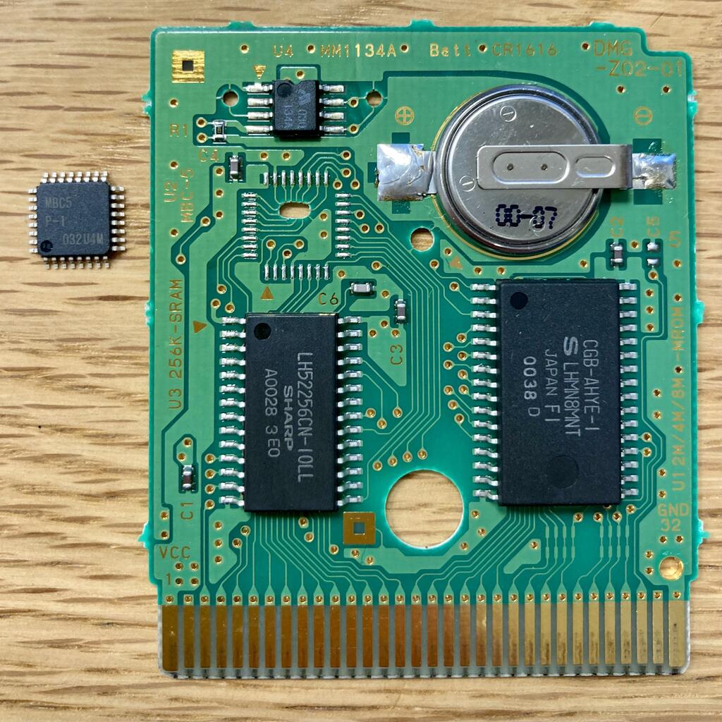
Here’s a photograph of a typical cart PCB that uses the MBC5 chip
(specifically, Super
Mario Bros. Deluxe), to help orient you as we discuss the individual
components below:
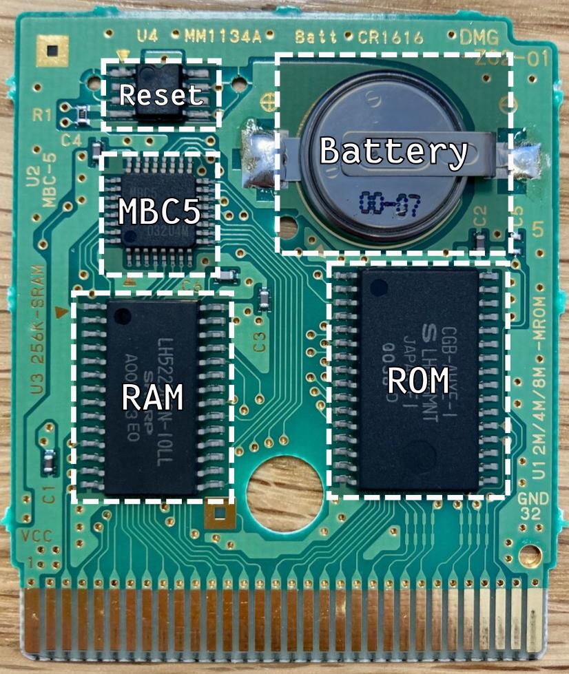
Let’s talk about ROM bank switching first.
ROMs and banks
I mentioned just now that MBC5 ROMs can store up to eight megabytes of data. However, the Game Boy itself can only address 64kB of memory. (It has a 16 bit address bus; 216 is 64kB.) And, in fact, since the Game Boy uses one whole bit of its address space to tell the ROM chip whether it should be on or off, there are actually only fifteen bits of addresses available to access data in the ROM (215 is 32kB). So what gives?
Here’s what gives. A ROM chip on a cart with an MBC5 might have (up
to) 23 address pins (223 is
8MB). However, only the bottom fourteen
(A0–A13) of those pins are directly connected
to the Game Boy’s address bus. The ROM chip gets values for the rest of
its address pins from the MBC5 chip. Here’s a simplified
diagram of the situation, showing only the components and connections
relevant to ROM bank switching. (In the diagram, boxes are components;
ovals label connections between those components.)

Okay, I know I said that this was a simplified diagram of the situation. I hope it will be a useful visual aid as we progress through this section, but I admit that, at first glance, it’s pretty damn complicated. The key thing to pay attention for now to is where the ROM chip is getting its address from. The Game Boy only sets the bottom fourteen bits of the address. The rest of the address is set by the MBC5 IC.
| ROM Address pins | Source |
|---|---|
A22–A14 |
MBC5 |
A13–A0 |
CPU |
This means that the Game Boy can only actually affect the lower
fourteen pins of the address bus. Effectively, the Game Boy can only
address and access 16kB of the ROM at any one time (214 is 16kB). But which
16kB of the ROM depends on what value the MBC5 puts on those upper
address lines (i.e., the ROM chip’s A14 through
A22 pins). If all of those address lines are set to zero,
then the Game Boy’s address space corresponds with the 16kB starting at
address 0x000000 in the ROM chip. If, say, those address
lines are set to 19 (hexadecimal 0x13, binary
0b10011), then the Game Boy would see the 16kB starting at
0x4C000 (binary 0b00001001100000000000000,
including leading zeros to show all 23 possible bits of the
address).
This is the essence of memory banking: the Game Boy accesses a fixed address range, but different parts of the ROM data are made visible in that address range, by setting the ROM address pins out-of-band.
The MBC protocol
The only question is… how does Game Boy software tell the
MBC5 chip what value to put on those upper pins? Remember that
the only means that the Game Boy has to communicate with the cartridge
are what we mentioned above: the flow control pins (_RD,
_WR and _CS), the 16-bit address bus, and the
8-bit data bus. Somehow we need to repurpose these pins to not just
access data from a memory IC, but also to communicate instructions from
the Game Boy and the MBC5 chip about which memory bank should be
active.
I think the solution that the engineers of the time came up with for
this is pretty clever. You’ll notice in the diagram above that the MBC5
chip is connected to address pins A13 through
A15. It’s also connected to all eight bits of the data bus,
and the _WR pin. This is so the MBC5 chip can watch what’s
happening on those pins, and pick out pre-arranged patterns of access
(combinations of address values and data values) that tell it what value
to put on the upper address lines of the ROM chip. This is a kind of
simple “protocol” built into the MBC5 hardware.
The protocol works like this. Whenever pin A13 is high,
and pins A14 and A15 are low, and the
_WR pin is low, the MBC5 copies whatever value is on the
data bus into a small internal memory. From then on, whenever the Game
Boy tries to read data (_WR pin is high), and
A15 is low, A14 is high, and A13
is low, the MBC5 copies the value from its internal memory onto the
ROM’s upper address bits. If A15 and A14 are
low, then the MBC5 puts all zeroes onto the upper address bits.
Here’s a table that summarizes this information:
A15, A14, A13 |
_WR |
Address range | MBC5 action |
|---|---|---|---|
| 001 | 0 | 0x2000–0x3FFF |
read value from data bus, store in memory |
| 010 | 1 | 0x4000–0x7FFF |
write previously stored value to ROM
A14–A22 |
| 00x | 1 | 0x0000–0x3FFF |
set ROM A14–A22 to all zeros |
It all comes together like this:
- Writing a value to the data bus when
A15is low (i.e., the ROM chip is active) and the address bus contains any value with a 1 in bit 13 (i.e.,0x2000–0x3FFF) sets a ROM bank number, which the MBC5 chip remembers for later. - Reading the data bus when
A15is low and the address bus contains any value with a 1 in bit 14 (i.e.,0x4000–0x7FFF) will access the portion of the ROM beginning at the value of the ROM bank, multiplied by 16kB. - Reading the data bus when both
A15andA14are low (regardless of the state ofA13) accesses the 16kB of the ROM beginning at0x0000and ending at0x3FFF(i.e., the first 16kB of the ROM).
From the programmer’s perspective, the first 16kB of address space
(0x0000 through 0x3FFF) is fixed to the first
16kB of the ROM, but—by using this little protocol—you can instruct the
MBC5 to make any part of the ROM available in the next 16kB of
address space (0x4000–0x7FFF).
Let’s pause for questions
“Hey, wait a second,” I hear one of you saying. “If the write pin is
low, that means that the Game Boy is trying to write a value! If I
write a byte to an address like 0x2000, which is
right smack in the middle of the ROM address space, shouldn’t that,
like, write the value to ROM?” Yes! This is exactly what would
happen, except that ROM stands for “read-only memory.” You can’t write
to it (unless you’re using an EEPROM IC, like a flash memory chip—we’ll
talk about how that works later on in the document). What makes this
little protocol so clever, in my opinion, is that it re-purposes the
(otherwise useless) _WR-high ROM address space as a way to
communicate information to the memory bank controller.
“Okay fine, hotshot,” you retort. “How about this? Why not make the entire first 32kB of the address range swappable, instead of having one 16kB chunk always fixed to the same place in ROM? Or break it up into differently sized chunks, like four banks of 8KB a piece?” Yeah, they could have done it that way if they wanted to! The bank switching system on the Game Gear/Sega Master System (which also has a 16 bit address bus) gives the programmer access to three 16kB banks, each of which can be mapped to arbitrary 16kB-aligned offsets in the ROM. There are also exotic Game Boy cartridge MBCs that split up the memory map in different ways, allowing access to several swappable 8kB ROM banks. The Intel 8086 processor has its own weirdo method for swapping different bits of memory into the memory map. So it’s not inevitable that the MBC5 would be designed to work the way that it does. That’s just the way the engineers decided it should work.
“One last question. In all of the rows in the table up there,
A15 is low (0). So why is A15 even connected
to the MBC, if its state isn’t being used as part of any functionality?”
Also a good question! Let’s talk about that next.
Cartridge RAM
It’s finally time to talk about on-cartridge RAM!
As previously mentioned, many Game Boy cartridges have a RAM chip on them. Most games use the on-cartridge RAM to store saved games: when connected to a battery, the RAM chip will retain its values even after the Game Boy is turned off, and the game can read those values when the player starts the Game Boy back up again. Technically, though, a Game Boy programmer can use the on-cart RAM for any purpose that they would use the internal RAM. Super Mario Land 2 uses it to hold level maps; Pokémon Red and Blue use it as a temporary scratchpad for decompressing sprite data.
Every commercial cartridge with RAM (that I’ve seen?) uses an MBC to
mediate access to the RAM. The cartridge RAM IC’s _CS1 (or
_CS) pin is connected to the MBC—not the address bus or
flow control pins—which then activates and deactivates the chip under
certain conditions (which we’ll discuss below). However, address pins
A0 through A12 from the address bus
are connected directly to cartridge RAM, as is the data
bus.
Here’s a diagram of the general situation, showing only the
connections that are relevant to cartridge RAM:

You may have noticed that there’s a similarity between how the top address lines of the on-cartridge RAM are connected to the MBC, and how the top address lines of the ROM are connected to the MBC. That’s because the MBC makes it possible to do bank switching on the cartridge RAM as well, using a method that is very similar to how ROM bank switching is accomplished. We’ll discuss this a bit later on.
You may have noticed that there’s a similarity between how the top address lines of the on-cartridge RAM are connected to the MBC, and how the top address lines of the ROM are connected to the MBC. That’s because the MBC makes it possible to do bank switching on the cartridge RAM as well, using a method that is very similar to how ROM bank switching is accomplished. We’ll discuss this a bit later on.
Now, it would be possible, technically, to connect the on-cartridge
RAM directly to the address bus and data bus, in the same way
that the cartridge ROM and the internal RAM are, instead of using the
MBC as a go-between. For example, the engineers at Nintendo could have
added another flow control pin specifically to enable/disable the
on-cartridge RAM IC, in addition to the _CS flow control
pin that we discussed earlier in the context of the Game Boy’s internal
RAM. Instead, the task of determining whether or not the cartridge RAM
chip should be enabled is delegated to the the MBC chip. It does this by
setting the cartridge RAM’s _CS1 pin high or low, depending
on certain conditions.
The right address range
The first condition that has to be met for the cartridge RAM chip to
be active is that the access needs to be in the correct memory
range. In particular, the part of the memory map that is
conventionally assigned to the on-cartridge RAM is
0xA000–0xBFFF. It so happens that every
address in this range begins with 0b101 (i.e.,
A15 is high, A14 is low, and A13
is high). So one of the things that the MBC does is check
A15, A14 and A13 to see if their
values match 0b101. If there’s a match, and the
memory is unlocked (see below), the MBC lowers the cartridge RAM’s
_CS1 pin so it can read from and write to the data bus.
Here’s a table summarizing what we know so far about what states of
A15, A14 and A13 are meant to
correspond to which memory chips being active (again, leaving out video
RAM, which is its own thing):
A15, A14, A13 |
Active chip | Address range |
|---|---|---|
| 00x | ROM | 0x0000–0x7FFF |
| 101 | Cartridge RAM | 0xA000–0xBFFF |
| 110 | Internal RAM | 0xC000-0xDFFF |
You can see that the Nintendo engineers figured out a way to nicely divide the memory map into distinct regions for each memory IC, using just three address pins. You can also see that this arrangement leads to both the cartridge RAM and the internal RAM having 8KB of addressable space, rather than the 32KB reserved for the ROM—which makes sense, since the internal RAM IC of (pre-Color) Game Boys is an 8KB chip, and most Game Boy games that shipped with on-cartridge RAM also used an 8KB RAM IC.
Locking and unlocking RAM
There is a wrinkle, however. As I alluded to previously, the MBC5 has
an internal bit that stores whether or not cartridge RAM access is
locked or unlocked. Even if the current memory access
is in the correct address range, the MBC5 will keep the cartridge RAM’s
_CS1 pin high (i.e., disabled) if that internal bit
indicates that cartridge RAM access is in the “locked” state. The MBC5’s
locked/unlock bit defaults to locked when the Game Boy starts up, and
the programmer can change it using another little bit of the MBC5
protocol.
In particular, the MBC5 waits for any access where the
_WR pin is low, and A15, A14 and
A13 are also all low (this corresponds to addresses
0x0000–0x1FFF). Then it checks the data bus.
If the data bus has 0b1010 (hexadecimal 0xA)
in its least significant four bits, the MBC5 changes the value of its
the locked/unlocked bit to unlocked. If the data bus has
any other value, then the MBC5 changes the bit to
locked. (All of this is part of the MBC5 protocol.)
In table form:
A15, A14, A13 |
_WR |
Data bus | Resulting lock state |
|---|---|---|---|
| 000 | 0 | XXXX1010 | unlocked |
| 000 | 0 | (anything other than XXXX1010) | locked |
And here’s a table that shows the value of the MBC5’s connection to
the _CS1 pin of the cartridge RAM, according to the
locked/unlocked bit and the current state of A15,
A14 and A13:
A15, A14, A13 |
Lock state | _CS1 |
|---|---|---|
| 101 | 0 | 0 (cartridge RAM enabled) |
| XXX | 1 | 1 (cartridge RAM disabled) |
| (anything other than 101) | X | 1 (cartridge RAM disabled) |
The question arises: why bother with this lock/unlock business at all? I’ve looked at a bunch of disassembled commercial game ROMs from the Game Boy’s heyday, and it looks like most games keep the cartridge RAM chip locked most of the time, and unlock it just long enough for one operation (e.g., storing a save file) before locking it again. The concern seems to be around save game integrity. If the cartridge RAM chip is enabled when there’s a power fluctuation—e.g., when the Game Boy is being turned on or off, or if the player removes the cartridge from the Game Boy when it’s turned on, or, I dunno, gamma rays or something—the contents of the chip could easily be corrupted. Better safe than sorry.
Banking RAM
The window in the memory map allocated to cartridge RAM is just 8kB
(0xA000—0xBFFF), but some RAM chips shipped on
commercial cartridges had up to 128kB of actual storage space. The MBC5
makes it possible to access all of that storage space, by providing a
way for the programmer to change which 8kB window of the actual RAM
storage is accessible in the memory map. This is bank switching, but
this time for the cartridge RAM.
The way that the MBC5 does this is broadly similar to ROM bank
switching, discussed above. Only address pins
A0–A12 are directly connected to the cartridge
RAM chip. Any of the RAM chip’s address pins higher than that are
connected to the MBC5 instead. Here’s the diagram showing the
connections between the Game Boy, the MBC5 and the on-cartridge RAM chip
again, to refresh your memory:
The biggest difference between cartridge RAM bank switching and ROM bank switching is that RAM banks are only 8kB, not 16kB, and correspondingly the number of address pins directly connected to the RAM chip is fewer (thirteen instead of fourteen; 213 is 8kB). Another important difference is that there is no fixed cartridge RAM bank. The entire range is swapped out when you change banks.
As with ROM bank switching, there’s a protocol for telling the MBC5
which values it should put on the RAM’s top four address pins
(A13–A16). Whenever the _WR pin
is low, and the values of A15, A14 and
A13 are 0b010 (corresponding to addresses
0x4000–0x5FFF), the MBC5 chip takes whatever
value is on the data bus and copies it to the RAM’s top four address
pins. For example, writing the value 0x7 (binary
0b0111) to address 0x4000 will switch to RAM
bank seven, which is the part of the RAM chip’s storage beginning at
offset 7 × 8kB =
0x0E000. Here’s a summary table:
A15, A14, A13 |
_WR |
Address range | MBC5 action |
|---|---|---|---|
| 010 | 0 | 0x4000–0x5FFF |
read value from data bus, store in memory |
| 101 | X | 0xA000–0xBFFF |
write previously stored value to RAM
A13–A16 |
It should be noted that comparatively few commercially-released games actually use cartridge RAM bank switching! Most games shipped with an 8KB RAM chip on the cartridge, which can be exhaustively addressed without needing to switch banks.
MBC5 summary
At this point, we can put together a table that summarizes the MBC5 protocol (at least for ROMs up to 4MB):
A15, A14, A13 |
_WR |
Memory range | MBC5 action |
|---|---|---|---|
| 000 | 0 | 0x0000-0x1FFF |
clear locked bit if data bus equals 0xA
(0b1010); set locked bit otherwise |
| 00X | 1 | 0x0000-0x3FFF |
set ROM A14–A22 to all zeros |
| 001 | 0 | 0x2000–0x3FFF |
store value on data bus as ROM bank number |
| 01X | 1 | 0x4000–0x7FFF |
write ROM bank number to ROM A14–A22 |
| 010 | 0 | 0x4000-0x5FFF |
store value on data bus as RAM bank number |
| 101 | X | 0xA000–0xBFFF |
write RAM bank number to RAM A13–A16; if
locked bit is clear, set _CS to 0 |
Here’s a diagram of the relevant connections, this time including
components for both RAM and ROM:

If you’re programming in assembly language, communicating with the MBC5 is fairly straightforward. All you need to do is read and write from the aforementioned addresses:
    ; enable cartridge RAM
    ld a, $0A
    ld [$0000], a  ; technically, any address from $0000 to $1FFF will work!

    ; set ROM bank visible from $4000 to $7FFF
    ld a, 4
    ld [$2000], a  ; often commercial ROMs use $2100, but any address from $2000 to $3FFF will work

    ; set RAM bank visible from $A000 to $BFFF
    ld a, 2
    ld [$4000], a  ; any address from $4000 to $5FFF will work

    ; disable cartridge RAM
    ld a, 0  ; or you could do 'xor a' to save a byte and a cycle
    ld [$0000], 0  ; any address from $0000 to $1FFF will work; any value other than $A will work
A few more details
There are a few more things that we need to discuss about the components of a Game Boy cartridge that don’t fit into the discussion of the MBC chip. Let’s dig into these below!
Keeping the RAM safe
If you take another look at the labeled photograph of a typical cartridge that we discussed above, there are two components that we haven’t discussed yet: the battery and the reset IC. We’ll talk about the two of these together.
In the previous section, we discussed the on-cartridge RAM chip in some detail. To be a bit more specific, the kind of RAM chip you’ll find on most commercially-released cartridges is a static RAM (SRAM) IC with a parallel interface. Game Boy games generally use the on-cartridge SRAM to store saved games, high score lists, and other information that needs to be persistent between power cycles. Parallel static RAM is, in a lot of ways, a perfect way to store data persistently: it’s fast, and because you can connect it directly to the address and data buses, the programmer can access it like any other kind of memory.
With a few exceptions, nearly every Game Boy game that stored save game data used parallel SRAM, which is part of what makes supporting Game Boy saved games in emulators and bootleg hardware relatively straightforward. The situation is much more complex with the Game Boy Advance: while some GBA cartridges have on-board SRAM, others use FRAM, Flash, or EEPROM, all of which have different software interfaces.
The biggest problem with SRAM is, of course, that it is volatile storage: the IC needs continuous power in order to retain its contents. When the Game Boy is powered on, this is no problem, as the on-cartridge SRAM can get power from the Game Boy itself. When you turn the Game Boy off, however, an alternative power source is needed. Fortunately, most SRAM chips can retain their contents using very little power—typically on the order of microwatts. Game Boy cartridges supply those microwatts with an on-board lithium button-cell battery, which is generally able to keep the data in the SRAM safe for 10+ years.
The tricky part of battery-backed SRAM is managing the moment when the SRAM switches over from Game Boy power to on-cartridge battery power. When the Game Boy power goes off, there are two things we need to make happen quickly and simultaneously:
- Change the SRAM’s power source from the Game Boy to the battery;
- Disable the SRAM chip (by, e.g., holding its
_CS1pin high and/or itsCS2pin low)
Why does the SRAM chip need to be disabled? While the Game Boy is off (or, generally, while the cartridge is not connected to anything), the pins on the cartridge edge are “floating”: because nothing is actively setting the value of the pins, the SRAM chip might interpret random electrical fluctuations on the pins as 0s or 1s. This could could corrupt the data on the chip, which in turn might zap all of the monsters you’ve pocketed.
To handle these two tasks, Game Boy cartridges usually have a
(somewhat confusingly named) “reset IC.” Here’s a ) simplified diagram
that shows the reset IC and its relevant connections:

The reset IC is connected to two power sources: the Game Boy’s 5V
power output, and the battery’s power output (typically 3V). The reset
IC is also connected to SRAM IC’s _CS pin. When the reset
IC is getting 5V from the Game Boy (i.e., when the cartridge is plugged
in and the Game Boy is on), the reset IC sends the Game Boy’s 5V power
to the SRAM chip. In this state, the reset IC also “forwards” the value
of the MBC5’s _CS pin to the cartridge RAM’s
_CS pin. By “forward,” I mean that whenever the MBC sets
the _CS pin low, the reset IC sets its own _CS
output low; whenever the MBC sets the _CS pin high, the
reset IC sets its own output high.
But when the reset IC detects that the Game Boy’s voltage has gone
below a particular threshold (i.e., when the Game Boy is turned off, or
the cartridge is otherwise not powered externally), the reset IC
instantly switches the SRAM’s power source from the Game Boy to the
on-cartridge battery. Simultaneously, it disables the SRAM chip by
setting its chip select pin as appropriate (now ignoring the value from
the MBC). When the Game Boy’s voltage goes above that threshold
(i.e., when the Game Boy is powered on again), the reset IC switches the
SRAM’s power source from the battery to the Game Boy, and resumes
“forwarding” whatever value the MBC puts on its _CS output
pin to the SRAM chip.
In practice, the situation is a bit more complicated than this, but I hope you understand the basic gist. If you want more detailed information about the precise interactions between the reset ICs, MBCs, and SRAM chips that are on actual Game Boy cartridges, I recommend Bucket Mouse’s very detailed and friendly documentation on the topic.
On-cartridge peripherals
Cartridges often contain custom electronics to provide useful features beyond just data storage, and the way that software interacts with these custom electronics is often entangled with MBC chips and the MBC protocol. I’m going to discuss two examples: haptic feedback in rumble-enabled Game Boy games, and the real-time clock in MBC3. These are well-documented and fairly easy to explain examples, and we’ll also return to these examples in the next section when we’re discussing how to make your own Game Boy cartridge. If you want to dig into some of the more esoteric on-cartridge peripherals, I recommend Pan Docs on MBC7 (provides an integration with an accelerometer, used with Kirby Tilt ‘n’ Tumble) and the Game Boy Camera.
Rumble
A number of commercial Game Boy games shipped with a “rumble” feature. These games have a small vibration motor inside of the cartridge housing, which the software can control in order to give haptic feedback during gameplay. Probably the most well-known of these is Pokémon Pinball; you can take a look at the cartridge and PCB on the Game Boy Hardware Database. Rumble cartridges were designed in a very clever way, which made it easy for software to activate the motor without having to include any extra control hardware on the cartridge beyond what the MBC5 chip already provides.
Remember that the MBC5 chip has pins that are intended to connect
directly to the upper address pins of the on-cartridge RAM chip, and
that the state of these pins can be controlled by writing a value to the
data bus when the address bus has a value anywhere between
0x4000 and 0x5FFF (i.e., A15 is
low, A14 is high, and A13 is low). Cartridges
with rumble, however, do things a little bit different. On these carts,
the pin that would normally go from the MBC5 to the RAM chip’s
A16 pin is instead connected to the vibration
motor (via a small motor driver, which powers the motor from an
included AAA battery that is also connected to the cartridge). Here’s a
diagram of the setup, showing only the relevant parts:

From the programmer’s perspective, the result of this configuration is that setting bit 3 of the RAM bank number turns the motor on, and clearing that bit turns the motor off again. (Here’s what I believe to be the relevant bit of code in the Pokémon Pinball disassembly.) This doesn’t actually change the RAM bank number; it just causes the MBC5 to change the state of its output pin that is connected to the motor. Simple and effective!
The diagram above suggests that three address lines are connected
between the MBC5 and the cartridge SRAM IC, which implies that some
commercial games with rumble used up to 64KB of SRAM (three pins = eight
banks; eight times eight kilobytes = 64KB). I’m not actually sure if any
commercial games with rumble made use of that much SRAM, or in fact if
any rumble-enabled games made use of cartridge RAM banking at all.
Pokémon Pinball, for example, only has 8KB of on-cartridge RAM,
meaning that it’s impossible to switch RAM banks, and consequently the
A13–A16 output pins from the MBC5 chip on that
PCB are simply not connected to anything. There were a number of other
rumble-enabled cartridges that had
no on-cartridge RAM at all.
Real-time clock on the MBC3
There were a handful of commercially-released cartridge for the Game Boy that had real-time clock functionality. In the context of electronics, a “real-time clock” (RTC) is a device for keeping track of how much time has passed while the system itself has been powered off. (Often RTC functionality is provided by a discrete IC, accompanied by a crystal oscillator and a small battery.) You’ll find RTC functionality in the smash-hit Acclaim Software classic, Mary Kate and Ashley: Pocket Planner, and also in gen 2 Pokémon games, which is the reason that you can only catch Ariados at night (among other things).
Instead of integrating a third-party RTC IC on their cartridges, Nintendo opted to implement the RTC functionality directly into the silicon of one of their memory bank controller chips: the MBC3.
In terms of bank switching, the MBC3 works very similarly to the MBC5. But what’s interesting about the MBC3 is how it extended the MBC protocol to make it possible for Game Boy software to access the RTC functionality baked into the chip. I’m skipping over a few details for the sake of simplicity, so don’t use this section as an authoritative guide to how to interact with or implement a Game Boy cartridge RTC system—I’m just trying to get across the gist. In particular, you should check Pan Docs for the nitty-gritty, including the process of “latching” and the “day counter carry bit.”
The MBC3’s RTC has five data fields: the current second, the current minute, the current hour, the lower eight bits of the current day, and the upper bit of the current day. The MBC3 treats each of these fields as their own RAM bank, like so:
- Bank
0x8: seconds - Bank
0x9: minutes - Bank
0xA: hours - Bank
0xB: day count (lower eight bits) - Bank
0xC: day count (ninth bit)
To read one of these values, the programmer first needs to switch to
the corresponding RAM bank. The MBC3 uses the same system for RAM bank
switching as the MBC5: you write the desired bank number to the data bus
with any address on the address bus whose top bits are
0b010 (i.e., 0x4000–0x5FFF). If
the bank number is 0x8 or greater, the MBC3 makes no
changes to the cartridge RAM address lines under its control; instead,
it saves that bank number for later. When the range of a subsequent
memory access is in the cartridge RAM address range
(0xA000–0xBFFF), the MBC3 checks the current
RAM bank number; if it’s 0x8 or greater, it disables
the cartridge RAM chip then drives the data bus with the current
value of the RTC variable in question.
Here’s a diagram showing the connections relevant for the MBC3 RTC
data. (Note that the MBC3 also does bank switching for the cartridge RAM
and ROM chips in manner similar to the MBC5. I’m omitting the
corresponding components from this diagram so we can visualize the RTC
functionality a bit better.)

This process might seem bizarre to programmers who are not used to
working with Game Boy memory bank controllers, because the MBC3 drives
the data bus with the value of the RTC variable regardless of what’s
happening with the lower bits of the address bus. To the
programmer, this makes it look like the entire memory range
from 0xA000–0xBFFF is filled with exactly the
same value!
The situation for writing values to an MBC3 RTC variable is similar.
First, the programmer switches to the RAM bank number corresponding to
the variable they want to change (with a write to
0x4000–0x5FFF). On a subsequent access, the
programmer drives the data bus with the new value for the variable, with
a value between 0xA000 and 0xBFFF on the
address bus. The MBC3, seeing the appropriate pin values on its address
pins, and seeing that the current bank number is associated with an RTC
variable, deactivates the SRAM chip and takes whatever value is on the
data bus and stores it in the corresponding RTC variable. Again, the
lower bits of the address bus don’t matter: writing to
0xBDEF will update the value just as well as writing to
0xA000.
“This is all very barbaric,” some of you might say. “Why not do
something sensible, like have the RTC seconds at 0xA000,
minutes at 0xA001, hours at 0xA002, etc.?” But
then some of you pause and think for a second. How would the MBC3 know
the difference between 0xA000 and 0xA001? It
would need to be connected to the A0 address pin! And to know the
difference between 0xA000 and 0xA002, it would
need to be connected to the A1 address pin. Before you know it, your MBC
is connected to almost half the damn address bus! Nintendo certainly
could have implemented it this way, but I guess they thought it
would be overly complicated, at least from a hardware standpoint.
There’s a particular strategy at play here, which is the use of
extensions or variations on the MBC protocol to make on-cartridge
peripherals accessible in the 0xA000–0xBFFF
range of the Game Boy’s memory map. We see this strategy in use not just
on the MBC3, but also the MBC6, MBC7, HuC1 and HuC-3. However, there’s
nothing preventing the custom cartridge designer from deploying their
own strategies to communicate between Game Boy software and weird stuff
on their cartridges, as we’ll see in a bit.
Making a Game Boy cartridge from scratch
To summarize, here’s what we’ve learned so far:
- The Game Boy CPU connects to many different memory ICs, and these ICs’ ability to read and write from the data bus choreographed through a combination of address pins and flow control pins.
- On-chip custom ICs, called “memory bank controllers,” make it possible to switch different segments of memory into the Game Boy’s memory map by changing the upper address lines of on-cartridge memory chips (ROM and RAM).
- Software communicates with MBCs using a kind of “protocol” consisting of patterns of memory access.
- The MBC and other on-cartridge components are charged with the important responsibility of maintaining the integrity of on-cartridge battery-backed RAM, both through software (RAM locking) and hardware (the reset IC).
- Hardware peripherals can be included on cartridges, and their functioning is often tangled up with the MBC chip or MBC protocols.
So what if you wanted to make a Game Boy cartridge from scratch? What exactly would you need to do? I’m assuming a few goals for our custom cartridge. Our cartridge should:
- Prefer off-the-shelf parts whenever possible (i.e., avoid using parts harvested from commercial cartridges);
- Be rewritable (i.e., it should use something like flash memory instead of a ROM chip, so that we can write ROMs to it multiple times);
- Support a reasonably large subset of the Game Boy library, not including software that uses on-cartridge peripherals (i.e., it should support multiple RAM and ROM banks, and potentially multiple MBCs)
Note that this section is not a tutorial on how to make a cartridge from scratch. Instead, think of it as an anthology of strategies to help you overcome potential stumbling blocks on the road to making a cartridge from scratch, along with facts that might be non-obvious to people who are approaching the problem for the first time. In particular, we’re not going to discuss things like PCB layout, or specific components, or the technical details of programming an MBC emulator. For information on those topics, I would invite you to learn from the bootleg cartridge I designed, including the documentation in the ABC PCB repository and the ABC firmware repository.
Also note that we’re going to focus on cartridges that use parallel flash to store ROM data, and that are intended to be used with a cartridge flasher. I wish I could talk authoritatively about cartridges that read ROMs from external media, like an SD card (e.g., the EZ-Flash Jr), but I’ve never done that before. I’d recommend the source code and documentation of the Croco Cart as a good place to start learning about that kind of cartridge!
The simple case: 32KB
Let’s go back to the “simplest possible scenario” diagram from a few
sections ago, which describes cartridges like Tetris that have
no on-cartridge RAM, no peripherals, and no more than 32KB of ROM (i.e.,
no need for ROM bank switching):
Creating a custom cartridge that only supports 32K ROMs is actually
fairly straightforward, and Game Boy hobbyists have been making
cartridges
like
this for ages. The simplest possible scenario is simple enough that
you can fairly easily make a Game Boy cartridge just by soldering a 5v
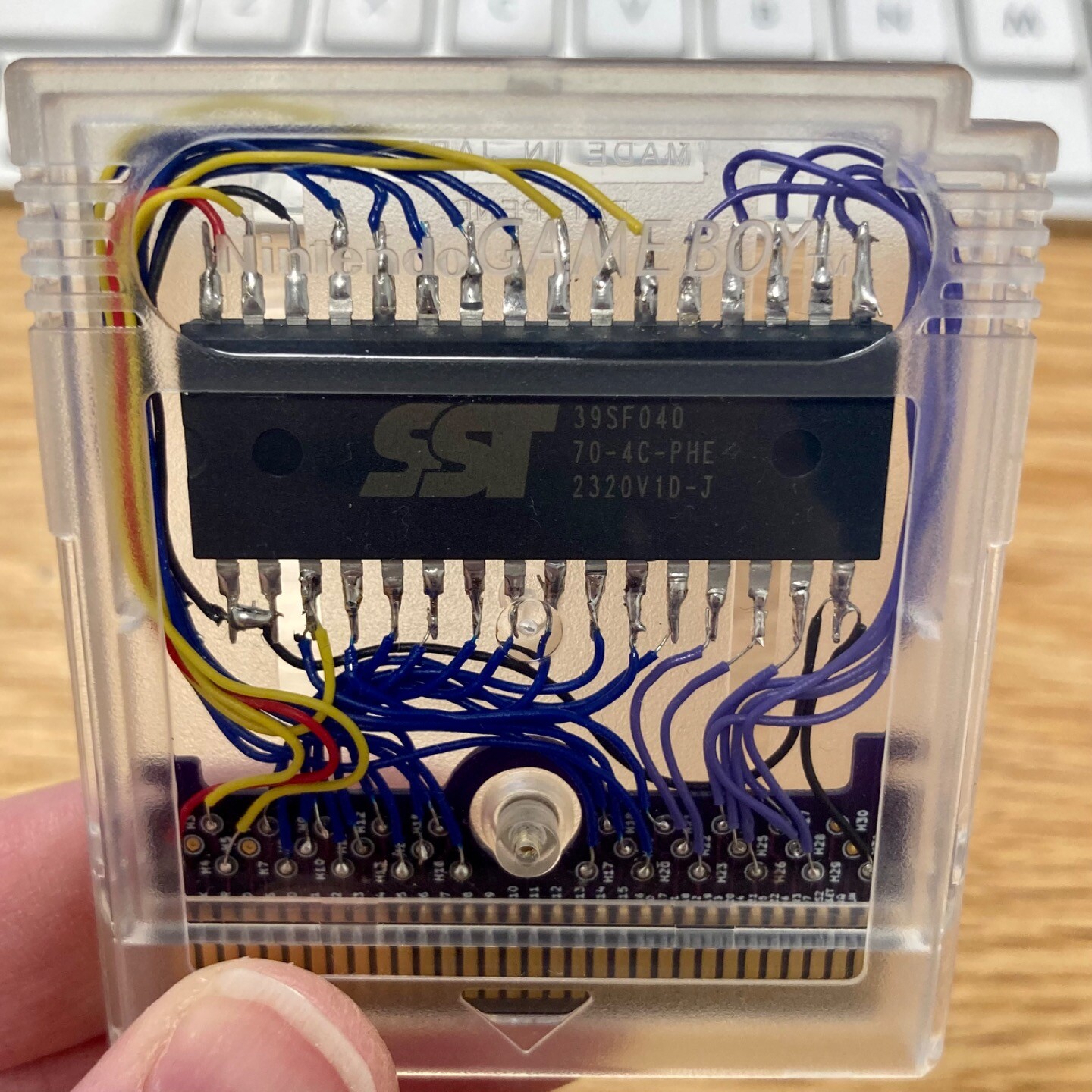
parallel flash IC to the cartridge edge, like I did with my first custom
cartridge:
The reason this works is that memory IC design is fairly well
standardized, and the Game Boy was designed to connect to off-the-shelf
memory ICs that follow this standard (as long as the voltages, timing
parameters, and bus width match up with the Game Boy’s requirements).
You connect pin A0 of the Game Boy’s address bus to pin
A0 of the memory IC, pin A1 of the Game Boy’s
address bus to pin A1 of the memory IC, and so forth,
including the data bus and (if it’s a ROM chip) connecting
A15 of the address bus to the chip’s _RD pin,
so that the ROM chip is only active when the access is in the
appropriate address range (as discussed at length above).
Using flash memory
Commercial Game Boy cartridges used custom fabricated read-only memory ICs to store their code and assets (mask ROM), which cannot be re-programmed. If you want a Game Boy cartridge that you can reprogram, you need to use a memory IC whose contents can be erased and then re-written, and that retains the new data until the next time you change it. We’ve already looked at one such memory IC—battery-backed SRAM—but this is not a popular solution for this use case, presumably because the game data would vanish when the on-cartridge battery runs out, which would be a bummer. (Though insideGadgets has some tantalizing if impractical prototypes with SRAM and FRAM.)
The flash IC
Instead, most third-party reprogrammable cartridges use parallel
(NOR) flash
memory, a kind of electrically erasable
programmable read-only memory (EEPROM). Below you’ll find the pinout
diagram of the parallel flash memory IC that I used in my 32KB
cartridge. (A “pinout” is a diagram of the chip that shows the names of
each of the IC’s pin, which you can then use as a way to look up what
that pin does. This diagram is from the memory IC’s datasheet.) Even if
you’ve never looked at a pinout of an IC before, some of this should
look familiar, just based on what you’ve learned from this document so
far! You can recognize the address pins, at least (A0,
A1, A2…). There are a few variations in how
I’ve been referring to typical memory IC pins in this document and how
the pinout labels those pins, namely:
VSSis ground,VDDis positive voltage (5V in this case)- Pins
DQ0,DQ1,DQ2(etc.) in the pinout are data pins (which we’ve been callingD0,D1,D2…) WE#is the same thing as_WR,OE#(“output enable”) is the same as_RD, andCE#(“chip enable”) is the same as_CS
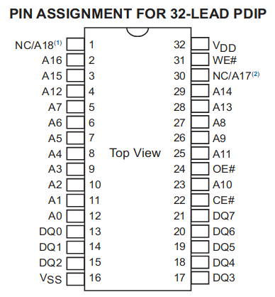
You can use this diagram to better understand how I did the wiring in my custom 32KB cartridge (shown above).
Note that this particular flash chip can actually store more than
32KB! Because I didn’t want to go through the hassle of supporting ROMs
greater than 32KB on my hand-soldered cart, I soldered all of the unused
address pins (A16, A17, A18) to
ground—essentially locking those address pins to zero.
The flash protocol
So how does the Game Boy actually interact with a parallel flash IC?
For read operations, parallel flash ICs work pretty much exactly like
their mask ROM or SRAM counterparts. You set the address pins to the
address of the value that you want to read, set _WR high,
_CS low, and _RD low, and then read the value
of the byte off of the data bus.
Writing data to the flash memory IC is a different matter entirely, because flash memory is a bit tricky. You can change the value of individual bits in a flash memory chip, but the update process can only change a bit from 1 to 0. If you want to change a 0 to a 1, you have to erase not just that bit but the entire sector of memory in which the bit is located. (Sectors are usually 4KB to 64KB.) The erase operation changes all bits in the sector to 1.
This means that, unlike as is the case with an SRAM chip, you can’t update a byte stored in a flash memory IC simply by setting the address of the byte on the address bus and the desired value on the data bus—at least, not in a practical way. You first have to erase the sector that the byte is in, then rewrite the sector with the updated value for that byte. Or you could simply erase the entire chip, and then rewrite the chip with an updated version of the data that had been on there previously. It’s kind of a hassle!
It is possible to introduce a layer of abstraction between the flash memory IC and the programmer that makes working with the flash memory more like working with regular files. A flash memory controller is a solution that lives in hardware; littlefs is a software solution that is especially appropriate for microcontrollers. Unfortunately, the Game Boy needs to be able to directly address the memory byte-by-byte, without a go-between, so we can’t use memory controllers or filesystems as drop-in solutions. We gotta wrangle that data the old fashioned way.
So there are at least three different operations we need to do to work with flash memory: read, write and erase. To facilitate these operations, flash memory ICs typically define a protocol for issuing commands that instruct the internal logic circuitry of the IC to perform those operations. The programmer issues these commands by setting the address bus and data bus to sequences of pre-determined values, in a particular order. (It’s a little bit like how an MBC works, actually!)
Each flash memory vendor has a slightly different protocol for these operations. To discover how to write and erase data on whatever flash IC you’re working with, you need to consult the datasheet. For example, according to the SST39SF series datasheet, the sequence of bus actions necessary to erase the entire chip consists of these steps:
- Write
0x5555to the address bus and0xAAto the data bus - Write
0x2AAAto the address bus and0x55to the data bus - Write
0x5555to the address bus and0x80to the data bus - Write
0x5555to the address bus and0xAAto the data bus - Write
0x2AAAto the address bus and0x55to the data bus - Write
0x5555to the address bus and0x10to the data bus
Whereas the sequence for setting the value of an individual byte looks like this:
- Write
0x5555to the address bus and0xAAto the data bus - Write
0x2AAAto the address bus and0x55to the data bus - Write
0x5555to the address bus and0x80to the data bus - Set the address bus to the address of the byte you want to set, and write the desired value of the byte to the data bus
An important thing to note is that the flash IC only matches the
state of (some subset subset of) the lowest bits of its address pins
when checking for commands. The SST39SF chips, for example, only
look at A0–A14 (i.e., addresses
0x0000 through 0x7FFF). The values on the
flash IC’s address pins above this range (A15,
A16, A17…) don’t matter, for the purposes of
determining whether a command is being issued. However, they do
matter in the last step of the byte-writing sequence, where the state of
all the address pins determines the memory location of the byte
written.
There are many other operations you can perform on a flash memory IC using this protocol (including handy things like getting the chip’s manufacturer ID, or its sector map), but if all you want to do is copy over a ROM, you really just need the erase operation and the write-byte operation.
So here’s where we are. We know that we can connect a flash memory IC
to a cartridge edge so that the memory IC’s address bus, data bus and
flow control pins align with their equivalents on the Game Boy. But then
we need some way to actually send data to that cartridge, by
issuing the necessary bus commands in accordance with the manufacturer’s
pre-defined protocol. And if we want to put our own software on the
cartridge, we’ll probably want to be able to copy a file from a computer
to the flash memory IC on the cartridge. Basically, we need the magical
device seen in this diagram:

“But where, oh where, might one find such a fantastical device,” I hear you lament. “Surely it cannot exist, not in this sinful, fallen world.” Ah, my friend. You musn’t despair! This magical device does exist, and it’s called a cartridge flasher. We’ll talk about cartridge flashers in the next section!
Observant readers may notice that the address bus values of the flash
memory commands are in ranges that are recognized by the MBC5 protocol.
E.g., the address 0x5555 is in the range
0x4000–0x5FFF, which is the range for updating
the RAM bank. The address 0x2AAA is in the range
0x2000–0x3FFF, which is the range for updating
the ROM bank. Eventually, we want our bootleg cart to emulate memory
bank controllers like the MBC5, so the question then arises: how the
cartridge can distinguish between bus operations intended for the flash
chip and bus operations intended for the MBC? We’ll discuss this when
the time comes!
Cartridge flashers
A cartridge flasher is a device that has a connection to a computer
on one end, and a connection to a Game Boy cartridge on the other. The
purpose of the device is to make it possible to write a file from the
computer to the memory ICs on the cartridge. (Usually, cartridge
flashers also work as cartridge dumpers, i.e., they can read
data from the cartridge and copy it to the computer, which can save that
data as a file; they can also usually read and write from the
on-cartridge RAM chip.) There are a number of cartridge flashers out
there (BennVenn’s
Joey Jr, FunnyPlaying’s
BurnMaster, the Open
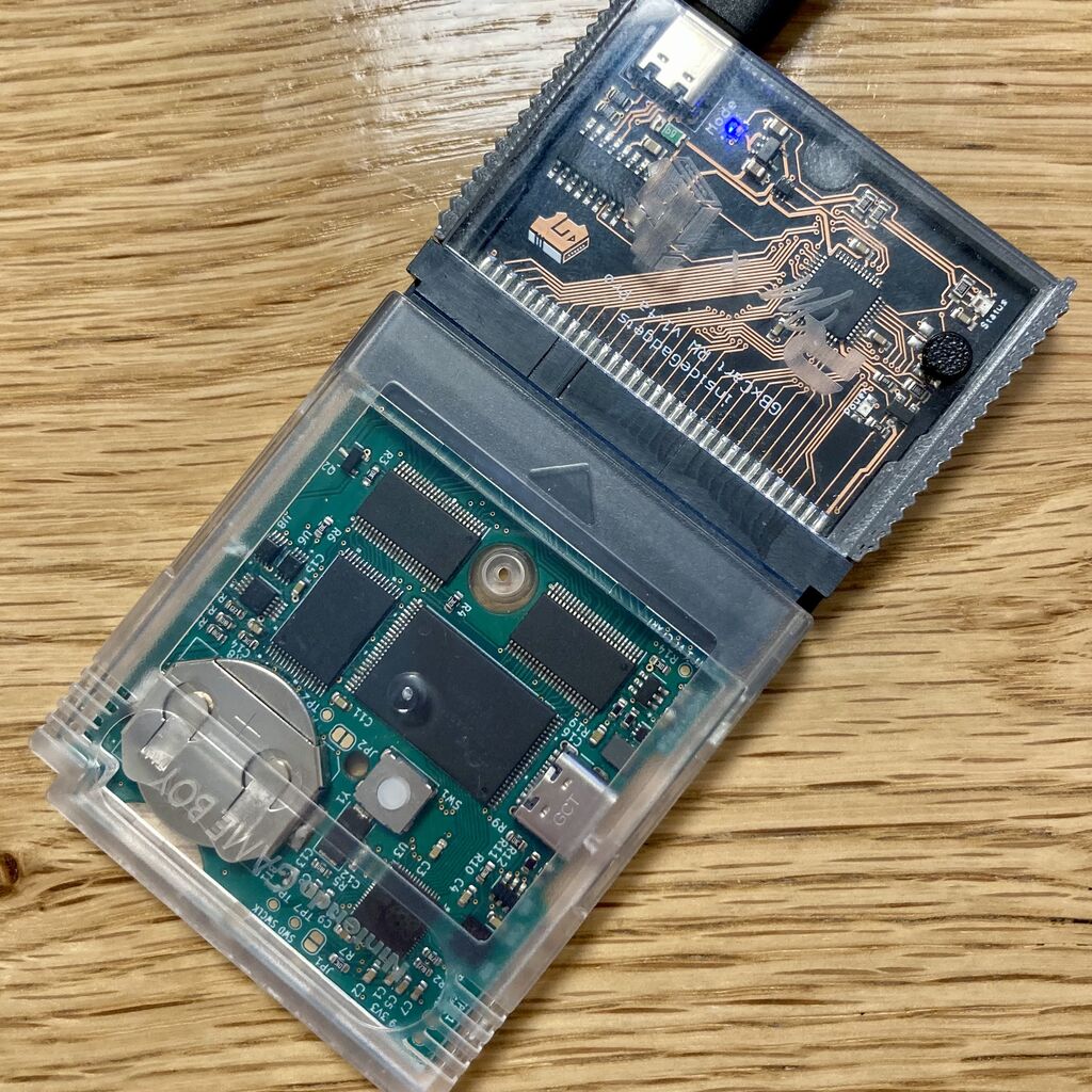
Source Cartridge Reader, etc.). But here’s a photo of my trusty GBxCartRW, which is the cartridge
flasher that I recommend. (The GBxCartRW is at the top of my photo. One
of my flash cartridges is plugged into it.)
Typically, a cartridge flasher has a USB port, which connects to the computer; the computer can then send data over the USB connection to a microcontroller on the cart. That microcontroller is connected, in turn, to a cartridge slot connector, which you plug your cartridge into. The microcontroller is what actually sets the flow control pins, the address bus and the data bus in order to read data from the cartridge and write data to the cartridge.
FlashGBX is software that you run on your computer in order to control the GBxCartRW. You can see configuration files for every supported flash cartridge in the FlashGBX source code repository, which include information on which commands to send to the flash memory IC on that particular cartridge (including the configuration file for a cartridge that uses one of the SST39SF series chips that we talked about earlier).
The FlashGBX source code also includes code for sending commands to MBC chips on the cartridge, so that the cartridge flasher can (e.g.) change the active ROM bank, in order to write ROMs larger than 32KB. Using a combination of the MBC protocol and the flash memory protocol, the cartridge flasher can read cartridge contents and write whatever data you want to the cartridge. Magic!
Emulating an MBC
Speaking of which, how do we support ROMs bigger than 32KB
on our bootleg cartridge? Well, we’ll do it the same way that Nintendo
did it: with a memory bank controller. More specifically, we need to add
something to the cart that “speaks” the MBC protocol, and can wrangle
the upper address lines of the on-cartridge flash and RAM chips so that
the correct slices of memory are available on the data bus when needed.
Basically, we need something that can do
everything that the MBC5 is doing in this diagram.
There are a handful of ways to do this! The simplest way is to sidestep the problem altogether and just harvest an MBC IC from an existing cartridge. And this isn’t a terrible strategy, especially if you have a cartridge whose MBC chip works fine but whose cartridge edge, ROM or SRAM are inoperative. Some Game Boy cartridges are collectors items, but millions of others are available for cheap and are ripe for the picking. Bucket Mouse’s flash carts all use MBCs and reset ICs harvested from original cartridges, and insideGadgets’ RTC cartridges have harvested MBC3 chips.
But let’s say you don’t want to sacrifice a commercial cartridge to the bootleg gods in order to satisfy your dark urges. While it’s possible to implement a subset of MBC behavior using discrete logic ICs, most flash cartridges out there use some kind of programmable logic device. Programmable logic devices are, essentially, a way to compactly implement complex configurations of logic gates on one chip, without the expense of manufacturing custom silicon. Generally, programmable logic devices are programmed in a hardware description language, such as Verilog or VHDL. I believe that insideGadgets’ MBC5-compatible cartridges use small CPLD chips to implement MBC5 behavior; BennVenn’s MBC3000 appears to use a CPLD chip as well. The EZ-Flash Junior has a big ol’ FPGA chip on it.
Still another way to do implement MBC behaior is to put a microcontroller on the cartridge, and program the microcontroller to respond to signals on the address and data bus and react appropriately. This is the approach that I took with my own bootleg cartridge, as well as the approach used on Shilga’s very cool Croco Cartridge and this Game Boy cartridge that uses an STM32 chip.
Deciding on which strategy to use really comes down to what your goals are. Harvested chips have few problems with compatibility, but to produce them at scale, you need to be able to source a bunch of old cartridges at low cost. FPGAs and CPLDs have a high ceiling in terms of speed and accuracy, at potentially higher cost and complexity than other solutions. I think microcontrollers are the most flexible strategy, but it’s difficult to make a microcontroller-based cart that is both highly accurate and doesn’t guzzle all your milliamps.
MBC protocol vs. flash protocol
At this point, there is a little problem that we need to discuss. It has to do with conflicts between what we need to put on the address and data buses to control the MBC, and what we need to put on the buses in order to control the flash IC. I want to spend a bit of time talking about this problem, because when I first started out I found it difficult to wrap my head around.
Regardless of whether we’re using a harvested MBC, an FPGA, or a microcontroller (or something else entirely), we need to implement a way for the cartridge flasher to read and write data beyond the first 32KB on the flash IC. The easiest way to do this is to use the machinery that we already have on the cart for dealing with this problem: the MBC itself. Let’s look at an example scenario to see how this would work, and potential complications that might arise.
An example scenario
Here’s an outline of the steps that a cart flasher might follow in order to write data to the cartridge flash memory:
- Load up some source file on the computer that the cartridge flasher
is connected to. We’ll call this
coolgame.gb. - Erase the flash chip entirely by sending the appropriate flash memory command.
- Copy the first 16KB of
coolgame.gb, byte-by-byte, to the memory range0x0000–0x3FFFon the Game Boy’s address bus, using the flash IC’s byte program command. - For each remaining chunk of 16KB in
coolgame.gb:- Use the MBC protocol to switch banks so that the next empty bank is
visible at
0x4000–0x7FFFon the Game Boy’s address bus; - Copy the next 16KB of
coolgame.gb, byte-by-byte, to the memory range0x4000–0x7FFFon the Game Boy’s address bus, using the flash IC’s byte program command.
- Use the MBC protocol to switch banks so that the next empty bank is
visible at
(There are other ways of going about this that are potentially
faster, but let’s stick with the simplest scenario for now.)
Let’s look at this sequence of events in terms of what values the
cartridge flasher is putting on the address and data pins of the
cartridge. Say that the cartridge flasher was writing the byte at file
position 0x8123 in coolgame.gb, whose value
happens to be 0x45. To write to this position in the
cartridge’s flash memory, the flasher first needs to switch ROM banks—in
this case, to bank 2. Then the flasher would use the flash IC’s “write
byte” command to write 0x45 to position
0x4123. We end up with the byte 0x45 at
address 0x8123 in the flash IC’s memory, which matches the
byte’s address in coolgame.gb.
If you’re having trouble following, let’s break it down a bit.
Remember that each bank is 16KB in size, or 0x4000 bytes.
In terms of the banks’ absolute addresses on the flash IC, bank 0 is
0x0000–0x3FFF, bank 1 is
0x4000–0x7FFF, bank 2 is
0x8000–0xBFFF, bank 3 is
0xC000–0xFFFF, and so forth. Switching to bank
2 causes the MBC to adjust the upper address pins of the ROM so that the
range 0x4000–0x7FFF on the Game Boy’s address
bus actually points to the absolute address
0x8000–0xBFFF in the flash, so writing a value
to 0x4123 on the Game Boy’s address bus actually
writes to the flash IC’s absolute address 0x8123. We’re
using the MBC to change the flash IC’s address pins behind the flash
IC’s back, but still using the flash IC protocol to write the actual
data.
Here’s what would happen on the data and address buses in this
scenario, assuming that we’d already erased the flash IC. In this
scenario (which, we shall see, doesn’t actually do what we want it to
do), imagine that the flasher holds the _WR pin low during
each write, and the _WR pin on the cartridge is connected
to both the _WR pin of the MBC and the _WR pin
of the flash IC.
| Step | Memory bus value | Data bus value | How the MBC interprets it | How the flash IC interprets it |
|---|---|---|---|---|
| 1 | 0x2000 |
0x2 |
switch to ROM bank 0x2 |
None |
| 2 | 0x5555 |
0xAA |
switch to RAM bank 0xAA |
Flash byte-program sequence, step 1 |
| 3 | 0x2AAA |
0x55 |
switch to ROM bank 0x55 |
Flash byte-program sequence, step 2 |
| 4 | 0x5555 |
0x80 |
switch to RAM bank 0x80 |
Flash byte-program sequence, step 3 |
| 5 | 0x4123 |
0x45 |
hold upper flash address pins so that Game Boy address
0x4000–0x7FFF points to the bank 2 area of the
flash IC |
Flash byte-program sequence, step 4 (our address and byte value) |
If you take a look in the bolded address values in the table above,
you should be able to see the problem. The MBC5 protocol dictates that
any write between 0x2000 and 0x3FFF should
change the current ROM bank. However, the flash protocol dictates that
you need to write to 0x2AAA as part of the byte-program
sequence… which has the side-effect of telling the MBC5 to set the ROM
bank! Because of this overlap, it seems like we simply won’t be able to
both switch banks using the MBC5 and issue the
sequence that the flash chip requires to program a byte value—unless we
only care about writing to ROM bank 0x55 (which would be
weird). How can we fix this?
Note that the required write to 0x5555 also
conflicts with the MBC protocol! In this case, however, because we’re
writing to the flash IC, we don’t necessarily care about spurious RAM
bank changes. If we need to read or write from RAM later, we’ll just
have to remember to reset the RAM bank to a known good value.
Flash and the MBC, living together in harmony
There are two ways to solve this problem. The first is easy: just
pick a flash memory IC whose commands don’t conflict with the MBC
protocol. The flash
IC that I use on my bootleg cartridge uses 0xAAA and
0x555 as command address values, instead of
0x5555 and 0x2AAA, meaning that the worst a
flash command can do is lock the on-cartridge RAM.
The second way is to use separate pins for the flash chip’s
_WR input and the MBC’s _WR input, so that we
can send commands to the two ICs separately. It so happens that there is
a pin on the Game Boy cartridge edge that was never
used for any commercial games: the AIN (or
AUDIO, or VIN) pin, which is right next to the
ground pin. Some flash cartridges repurpose this as a “substitute”
_WR pin. On such cartridges, the flash IC’s
_WR pin is connected to the MBC’s _WR pin (as
normal), but the flash IC’s _WR pin is connected to
AIN. This means that the flasher can lower AIN
for commands that are meant for the flash IC, but lower _WR
pin for commands that are meant for the MBC. Conflict resolved! Here’s a
diagram of what the situation looks like, including only the relevant
elements:

I don’t know who came up with this solution originally, but it’s very
clever! Essentially, we have two _WR pins: one for
the MBC (and on-cartridge RAM, if any) and one for the flash IC. As long
as the cartridge flasher is careful to never lower both pins at the same
time, the flash IC will never see the MBC commands, and the MBC will
never see the flash commands. Even if you’re using a flash chip whose
commands don’t conflict with the MBC, it still might be a good
idea to use this setup, just as an extra bit of protection against
accidentally writing incorrect values to flash memory. FlashGBX has
support for this strategy built in.
Cartridge RAM and data persistence
Blessedly, parallel SRAM ICs have none of the data access complications of parallel flash: you just set the address bus and read/write to the data bus. No protocol required. It’s even possible to purchase parallel SRAM that is more or less functionally equivalent to the SRAM ICs found on commercial Game Boy cartridges back in the day. Provided that your solution for emulating an MBC also supports all of the cartridge RAM-related portions of MBC functionality (locking/unlocking RAM, restricting access to particular address ranges, and bank switching for games that need it), the way you wire up your on-cartridge SRAM IC will look very similar to how it’s wired up on a stock cartridge.
Complications arise, however, when we start thinking about how to ensure that the data on the cartridge RAM is persistent between play sessions. We’ll talk about two strategies for doing this, both with benefits and drawbacks.
SRAM plus battery
The first strategy is to do as Nintendo did: use an on-cartridge battery. The main benefit of this solution is that SRAM is relatively cheap, and little button cell batteries are relatively cheap, and you can get impressively long retention times with this combination, even if SRAM is technically volatile memory. One drawback is that button cell batteries are fairly large, and so they take up space on the cartridge PCB that might otherwise be put to better use.
But the real trouble here, right off the bat, is making sure that the
SRAM switches cleanly between Game Boy power and battery power, without
risk of memory corruption. (We discussed this problem earlier in the
section on MBC5 and Cartridge RAM.) Ideally, we’d be able to buy an
off-the-shelf IC that works exactly like the reset ICs found on the
original cartridges: it switches between power sources based on voltage
levels, forwards an incoming _CS signal to the SRAM chip
when above that threshold, then holds the SRAM’s _CS pin
high when below that threshold. (Or equivalent functionality.)
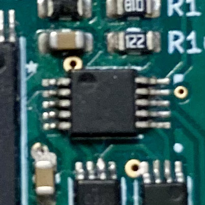
From what I can gather, there used to be a wide variety of ICs on the market that were designed especially for supporting battery-backed SRAM, and had exactly the functionality I just described. Nowadays, though, demand has waned and the least expensive single-chip solution out there is Texas Instruments’ TPS3613—and even that IC (as of this writing) costs an eye-watering US$4.45 at single unit prices (!). It would be possible to design a circuit with discrete parts (a voltage detection IC and a MOSFET or two, say) that would serve the same purpose and maybe be cheaper. But I think it’s better to be safe than sorry when it comes to save game data and battery life, so I opted to use this IC in my own cart design. (It is, by some margin, the most expensive part in my BOM. Oh well!)
I will once again direct you to Bucket Mouse’s excellent explanation of battery-backed SRAM on Game Boy cartridges for a more in-depth discussion, including information on which reset ICs are worth harvesting from original carts.
Ferroelectric RAM (FRAM)
The second strategy for persistent data storage is to do as Nintendid not: use some kind of non-volatile memory for saved games. The popular choice here is parallel ferroelectric RAM (or FRAM), as featured on various insideGadgets cartridges, FunnyPlaying’s Midnight Trace, etc. The interface of parallel FRAM ICs is exactly like the interface to parallel SRAM ICs (aside from some potential timing issues, depending on the IC in question), and in fact many FRAM ICs are sold as pin-compatible drop-in SRAM replacements. FRAM retains its contents for decades without external power, so there’s no need for a battery or a reset IC to switch power sources.
The main disadvantage of FRAM, and it’s a big one, is cost. As of this writing, you can get a 256Kbit (32KB) parallel SRAM chip for under US$1.50; a parallel FRAM chip with similar capacity costs around US$12. At those prices, you’re coming out ahead with SRAM, even with the added cost of the button cell and the TPS3613. Still, FRAM might give you the peace of mind that you need when it comes to the security of your pikachus.
Flash cartridges with SD cards, like the EZ-Flash Jr, use a third strategy, which is to copy the contents of the on-cartridge SRAM to the SD card, and then copy that data back into the SRAM when the cartridge starts back up. The benefit of this is, of course, that the saved game data is right there, safe and sound on your SD card. The drawback is that writing data to an SD card is typically very slow—much slower than the speed at which the Game Boy writes to RAM—so SD card-based cartridges can’t keep up with SRAM changes in real-time. The EZ-Flash Jr cartridge solves this problem with an on-cartridge button that the you have to press after they save their game. The button initiates the process of copying the SRAM contents to the cartridge. You just have to make sure that you wait a few seconds for the copy to complete before turning your Game Boy off.
Power problems
Like many other gadgets and gizmos released in the late 1980s and early 1990s, the Game Boy runs on 5V. Consequently, Game Boy cartridges run on 5V as well. Nowadays, however, most small electronics run at lower voltages internally—typically 3.3V, but sometimes even lower. So folks who make Game Boy cartridges from scratch have a choice to make when sourcing their parts: you can either find 5V components (like 5V flash memory and 5V SRAM)—which are becoming more rare and more expensive—or you can do some electronics gymnastics to convert the Game Boy’s 5V power and signals to a lower voltage, so you can use lower voltage components instead. In this section, we’re going to dive into what’s involved in implementing the second strategy.
If you want to use lower voltage components on your cartridge, you need two things:
- A voltage regulator to convert the Game Boy’s 5V power source to whatever voltage that can safely power your components;
- A logic level translator (or level shifter) to convert the Game Boy’s 5V logic signals (i.e., the values on the data bus and address bus) to a voltage that won’t fry your components’ inputs.
This diagram shows the general relationship of components when you
have both of these in place:

Let’s discuss voltage regulation and level translation in turn.
Voltage regulation
Broadly, there are two strategies for converting a high voltage power source to a lower voltage power source: burn off the excess voltage as heat with a linear regulator, or use a buck converter, which switches the higher voltage power source on and off very fast, so that the resulting voltage averages out to the desired lower voltage. (That’s very simplified explanation of a buck converter, but you get the gist.)
Both approaches have benefits and drawbacks. Linear regulator circuits are easy to design and inexpensive, but linear regulators themselves are not very efficient: in the case of a 5V to 3.3V conversion, at least 34% of the energy that flows through the regulator goes to waste—which can result in reduced battery life for the system as a whole. Buck converters are much more energy efficient, but they’re more complicated to design and more expensive (partially because of the increased number of components needed). A poorly designed buck converter circuit can also potentially introduce unwanted noise into the Game Boy’s electronics.
From the photos on the site, I’d bet that BennVenn’s MBC3000 uses a linear regulator. On the other hand, the EZ-Flash Jr has two buck converters—one at 3.3V and another at 1.2V—presumably because there are both 1.2V and 3.3V components on the cartridge. I opted for a buck converter in my own design.
I am not a paid endorser but if you’re working on a buck converter circuit, I highly recommend TI’s WEBENCH circuit designer tool. It’ll give you some confidence while you pick out that inductor.
Level translation
Level translation can also be tricky! The chief potential trouble with level translators is that their ability to produce clean output degrades as the speed of signal changes on the input increases. The Game Boy isn’t an especially fast processor, but the signals on the data and address pins can reach 4MHz, which means that some voltage translation solutions (like using a simple voltage divider) are probably not going to cut it.
Also, some level translators require external control of the direction of translation (i.e., whether the translator is transmitting data from high to low, or low to high), and external control of whether or not the level translator should be active at all. This means that the cartridge needs to incorporate some kind of logic that can make these determinations—which, as we’ve seen in this document, need to take into account a number of different factors (e.g., the address range, whether the cartridge RAM is locked or not, etc.). The task is complicated enough that you might need to include discrete logic ICs or a microcontroller in your cartridge design just for the purpose of controlling the level translator.
The good news is that there are a number of off-the-shelf level translators that get the job done with a minimum amount of fuss. I’ve used Nexperia’s 74ALVC164245DDG with some success on my own cartridge designs. I’ve seen folks use TI’s TXB0108 for this purpose as well, which has an automatic direction sensing feature that obviates the need for all of the direction logic that I mentioned above.
The bad news is that level translation ICs aren’t super cheap: TI’s non-bulk list price for one TXB0108 is (as of this writing) US$1.14, which means that implementing level translation for your cartridge’s address and data bus can adds a non-trivial amount to the cost of your cartridge’s bill of materials.
When I priced it out recently, it didn’t seem like there was a meaningful difference in the cost between using all 5V parts (which tend to be more expensive) versus using 3.3V parts along with a voltage regulator and level translator. Eventually I elected to use 3.3V parts, which makes my cartridge design more complicated, but also makes it (I think!) more future-proof.
Strategies for on-cartridge components
One of the exciting possibilities open to cartridge makers is the ability to include weird hardware components on the cartridge, in order do to things with the Game Boy that Nintendo never envisioned. A few examples of custom cartridges that do this:
- orangeglo’s Orange FM cartridge
- BULB! game with a cart incorporating an LED
- Game Boy cartridge with WiFi
- John Sutley’s World’s Worst Dash
- Peter Sobot’s Music Boy cartridge
- Anders Granlund’s Wolf (custom cartridge with “co-processor” for playing Wolfenstein 3D on the Game Boy Color)
I made a little light theremin with my own cart design, just as a quick experiment! It was fun.
A cartridge that integrates hardware components like this needs to have some way for the software on the Game Boy to communicate with the hardware. As you might expect, there are multiple ways to do this! Simple one-bit, one-way communication (e.g., to blink an LED, or to start/stop a rumble motor, as we discussed earlier) may just require connecting the hardware to a particular address pin on the hardware side, and then accessing an address that changes the value of that pin on the software side. The “Systems of Levers” channel on YouTube has a very clear tutorial about how to do exactly this which I highly recommend as a starting point.
More sophisticated communication scenarios might involve designating a particular address or address range in the memory map for writing data (Game Boy to cartridge) and another address range for reading data (cartridge to Game Boy). In this scenario, you’d need some logic (microcontroller, PLD, discrete logic, etc.) on the cartridge that detects that matching pattern of address values, and drives the data bus or reads from the data bus accordingly, taking care to ensure that no other components will be writing to the data bus at the same time.
In the “on-cartridge peripherals” section above, we saw a few
examples of how commercial cartridges handled this: they used the MBC as
a proxy, so that reads and writes in the cartridge RAM memory range
(0xA000–0xBFFF) are redirected to the
peripheral hardware under certain conditions. My own cartridge uses this
same address range to allow the cartridge software to communicate with a
microcontroller on the cart, in order to facilitate multicart
functionality; the Croco
Cartridge also uses this address range (although in the case of the
Croco Cartridge, the microcontroller is also serving the role of the
on-cartridge RAM, which means that this memory range is essentially
mapped to both the Game Boy’s memory and the memory of the
microcontroller on the cartridge—very slick).
The Game Boy WiFi cartridge I mentioned above uses a different
strategy altogether. There’s
a number of discrete logic ICs on the board connected to the address
bus that signal the on-board microcontroller when a particular addresses
are being accessed. When the address is 0x7FFF, the Game
Boy software is sending data to the microcontroller; when the address is
0x7FFE, the microcontroller is sending data to the Game
Boy. Using this convention, the on-cartridge microcontroller and the
Game Boy software can take turns driving the data bus to exchange
information.
Conclusion and additional resources
So here’s what we now know about making a cartridge from scratch:
- Parallel flash is a good match for the task of storing Game Boy ROMs on a cartridge, since the pinouts of parallel flash ICs are similar to the ROM chips on original cartridges
- Once the flash IC is on the cartridge PCB, you need some way to get data on there, which is why we have cartridge flashers
- Hardware “emulation” of an MBC IC can be implemented in various ways, including FPGAs and microcontrollers
- For storing persistent data, you have your choice between battery-backed SRAM or FRAM, both of which kind of suck (for different reasons)
- Potential sources of trouble include flash/MBC protocol conflicts and the need for voltage translation between the Game Boy and on-cartridge components
Thank you for reading! I hope I delivered on the promise of giving you more than you wanted to know on the topic of Game Boy cartridges. However, if your knowledge somehow remains below the threshold of your desire, here are some other resources that might finally get you over the top:
- If you want to study schematics of commercial cartridges, Martin Refseth’s reproduction cartridge PCBs are as close as you’re going to get!
- Also check out Bucket Mouse’s Game Boy Cartridge PCBs (adapted to use flash memory).
- System of Levers’ How Game Boy Memory Addresses Work is very clear and slightly higher-level explanation that has significant overlap with the content of this document. The channel also has a series of excellent hands-on examples of adding hardware peripherals to the Game Boy: How to control an LED with the Game Boy and how to read a button with the Game Boy.
- Gameboy DMG ROM and RAM Bank Switching is a helpful and clear narrative explanation of how memory banking on the Game Boy works, from the programmer’s perspective
- Very helpful timing diagrams of Game Boy memory access patterns
- And of course, Pan Docs and gekkio’s Game Boy: Complete Technical Reference.
License
The contents of this website are published under the CC BY-NC-SA license. Use of the contents of this website as part of a dataset to train a machine learning model is allowed, under the terms of this license. (For example, a model that includes this website as part of its dataset must explicitly credit me among its contributors, and must be distributed under the same license as the website itself. Also, any model making use of this website in its data set must not be used for commercial purposes.)
What's Your Reaction?
 Like
0
Like
0
 Dislike
0
Dislike
0
 Love
0
Love
0
 Funny
0
Funny
0
 Angry
0
Angry
0
 Sad
0
Sad
0
 Wow
0
Wow
0


